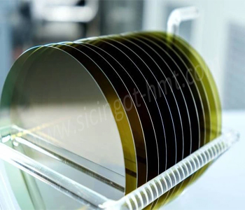
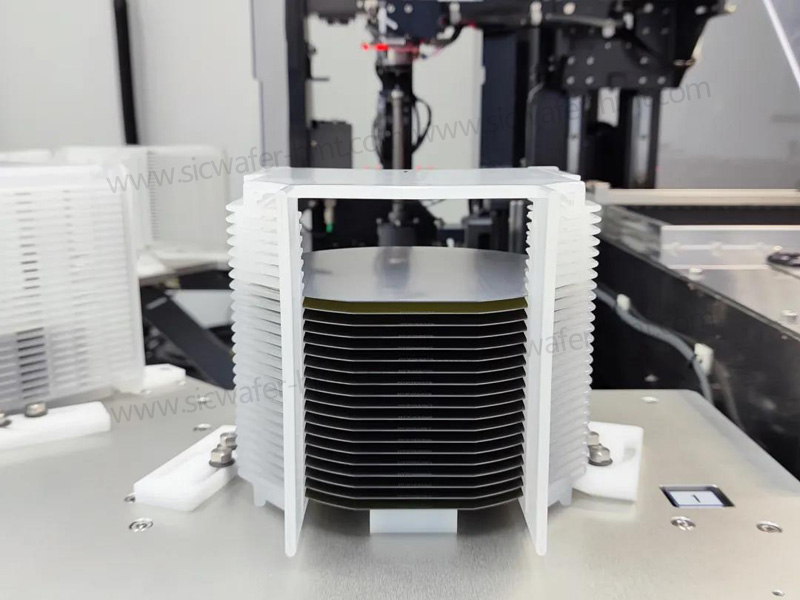
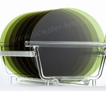
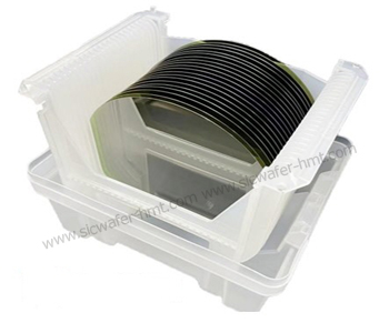
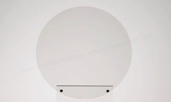
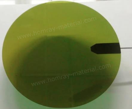
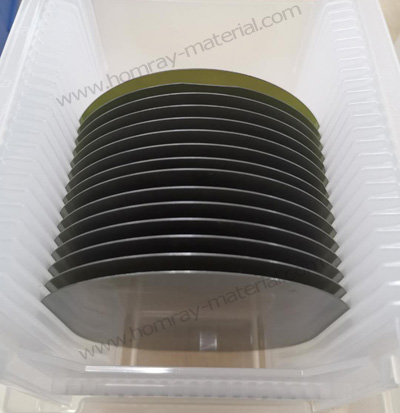
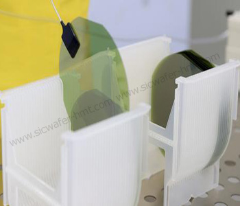
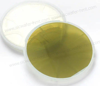
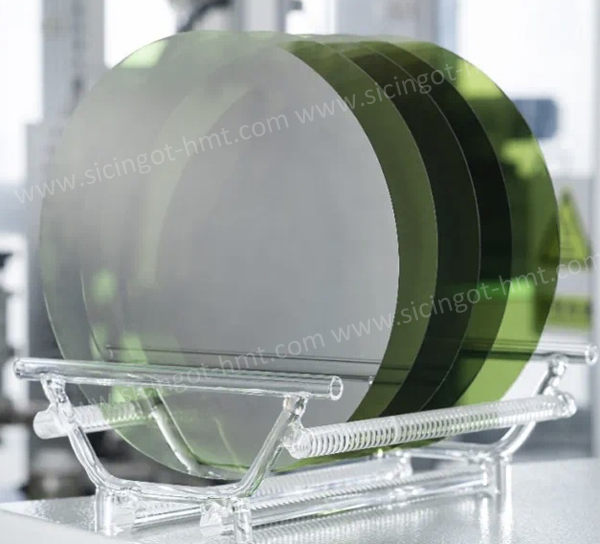
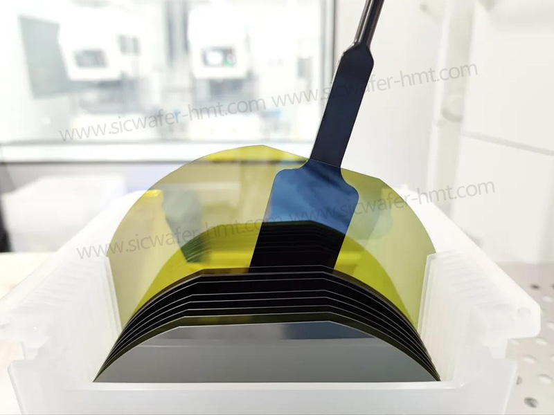
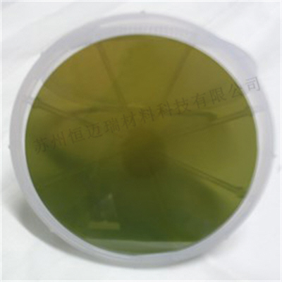
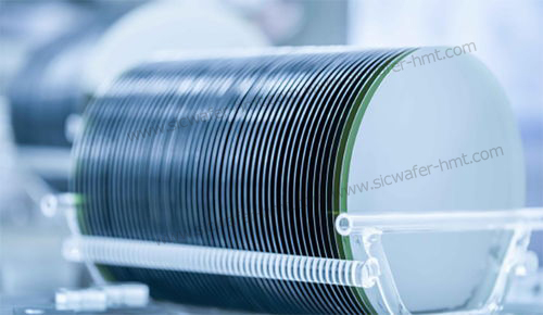
4''6''8'' SiC Wafer Producer Epi-Ready DSP
Grade: D/R/P Grade
Type: 4H-HPSI/4H-N
Dimension:2inch 4inch 6inch 8inch
Thickness:350±25um/500±25um
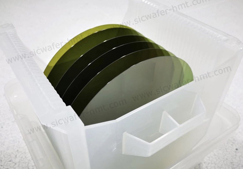
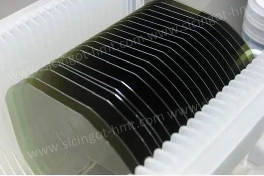
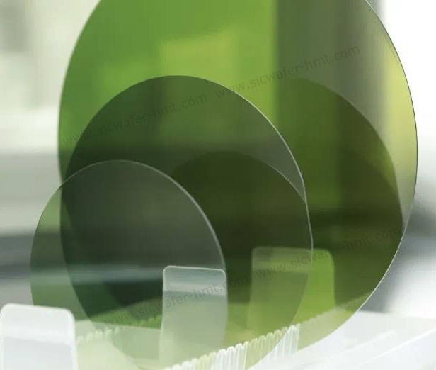
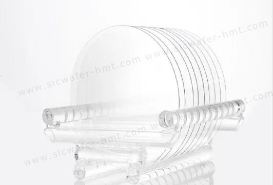
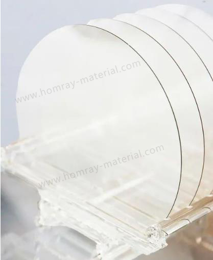
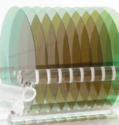
As a premier producer of silicon carbide (SiC) substrates, we deliver Epi-Ready Double-Side Polished (DSP) SiC wafers in 4'', 6'', and 8'' diameters, engineered for demanding semiconductor applications. Our wafers are tailored to streamline epitaxial growth processes, ensuring:
-
Industry-Leading Quality: Ultra-low defect density (<0.2 cm⁻²) and sub-nanometer surface roughness (Ra <0.5 nm).
-
Thermal & Electrical Excellence: High thermal conductivity (4.9 W/m·K) and breakdown field strength (2.8 MV/cm) for robust power device performance.
-
Polytype Versatility: Dominant 4H-SiC crystal structures, optimized for MOSFETs, Schottky diodes, and RF devices.
With the surge in demand for high-power, high-efficiency power supplies in audio systems, industrial equipment, medical instruments, and new energy applications, traditional silicon-based power devices are increasingly revealing limitations such as high-frequency losses, demanding thermal management, and bulky form factors. Silicon Carbide (SiC), with its wide bandgap (3.2 eV), high breakdown electric field (2.8 MV/cm), and superior thermal conductivity (4.9 W/cm·K), has emerged as a breakthrough solution to overcome these constraints. This article systematically analyzes the revolutionary value of SiC in high-power amplifier (HPA) power supplies from technical principles, application scenarios, performance comparisons, and future trends.
Technical Advantages of SiC Power Devices
1. High-Frequency & High-Efficiency Performance
SiC MOSFETs achieve switching speeds in the nanosecond range—over 10x faster than silicon-based IGBTs—with no reverse recovery current. For example, in LLC resonant topologies, SiC MOSFETs enable switching frequencies beyond 100 kHz, reducing magnetic component size by 50% while improving efficiency by 3%-5%. In server power supplies, higher frequencies (200 kHz+) further shrink magnetic components, achieving power densities exceeding 300 W/in³.
2. High-Temperature Stability & Reliability
SiC devices operate stably at 200°C+, with a junction temperature tolerance 100°C highe than silicon-based devices. In automotive amplifiers, SiC solutions reduce heatsink volume by 40%, while industrial-grade amplifiers demonstrate a <0.1% failure rate after 10,000 hours of continuous operation in -40°C to 125°C environments.
3. Low Loss & High Power Density
SiC Schottky Barrier Diodes (SBDs) feature a forward voltage drop of just 1.2 V, cutting conduction losses by 40%. Combined with low RDS(on) SiC MOSFETs, system efficiency exceeds 97%. In 100W audio amplifiers, adopting SiC SBDs boosts efficiency from 86% to 90.47% , with output ripple below 50 mV.
SiC power devices, with their high-frequency efficiency, thermal stability, and power density, are redefining the design paradigm for high-power amplifier supplies.From audio equipment and industrial power systems to medical devices and renewable energy applications, SiC solutions have demonstrated 3%-5% efficiency gains, 40% size reduction, and 5x longer lifespan. As 8-inch wafer technology matures and supply chain innovation accelerates, SiC is poised to become the mainstream choice for next-gen power amplifiers—ushering in a new era of ultra-compact, ultra-efficient power electronics.