
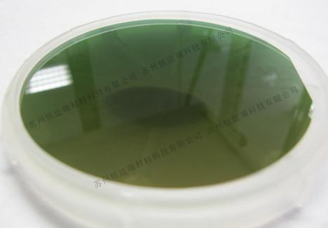
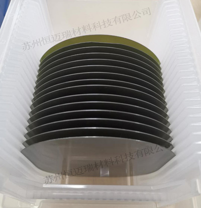
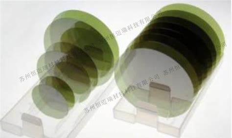
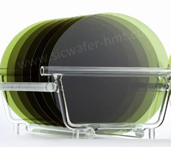
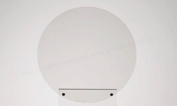
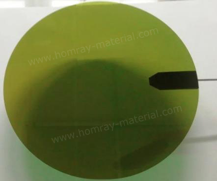
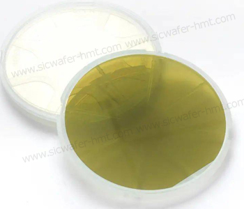
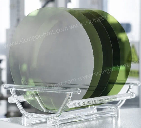
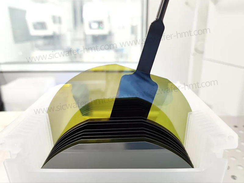
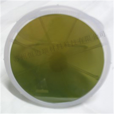
Low MPD 4 inch SiC Substrate Manufacturer
Dimension: 4 inch
Type: 4H-N
MPD: <0.5cm2
Grade:Production Grade
Product Description
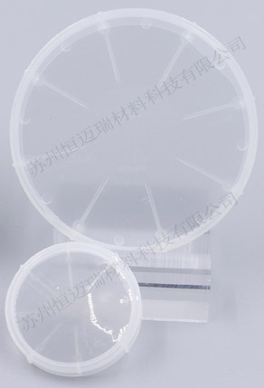
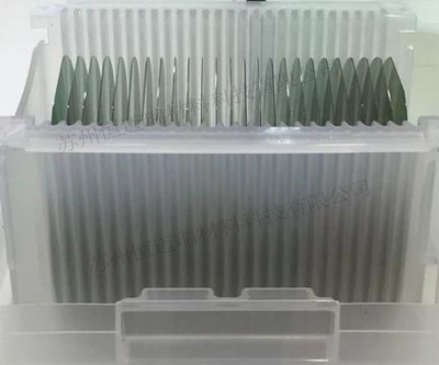
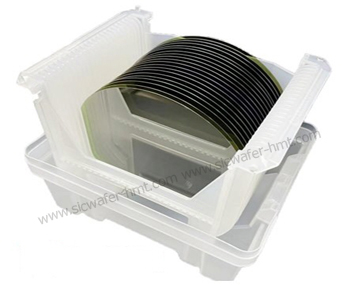
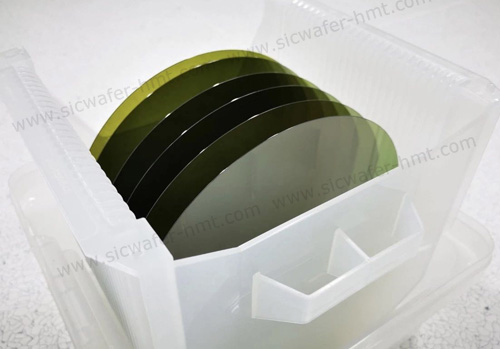
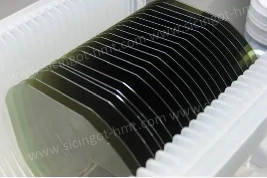
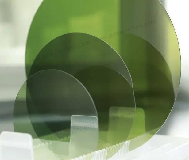
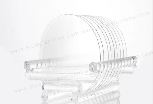
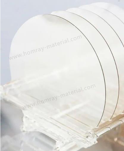
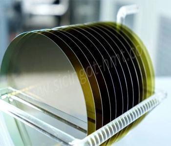
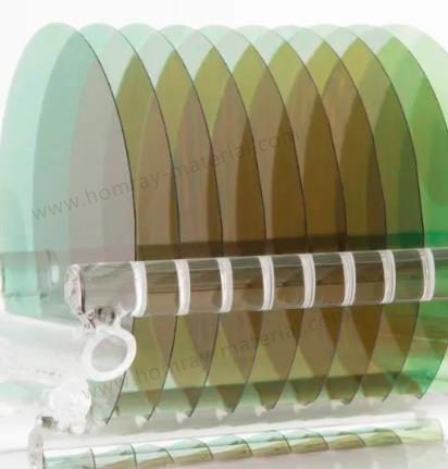
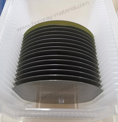
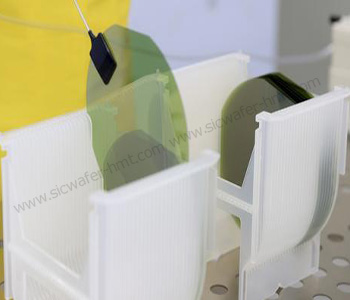
Purchasing low MPD 4 inch SiC Substrate from HMT company, we provide high quality 4 inch Silicon Carbide SiC wafer both D Grade and P Grade. We support customized SiC Wafer parameters,like thickness, LTV ,TTV etc..You can get preferential price for SiC Substrate in HMT even customzing. Not only 4 inch, We also proving 2 inch 6 inch and 8 inch SiC Substrate for worldwide customers.
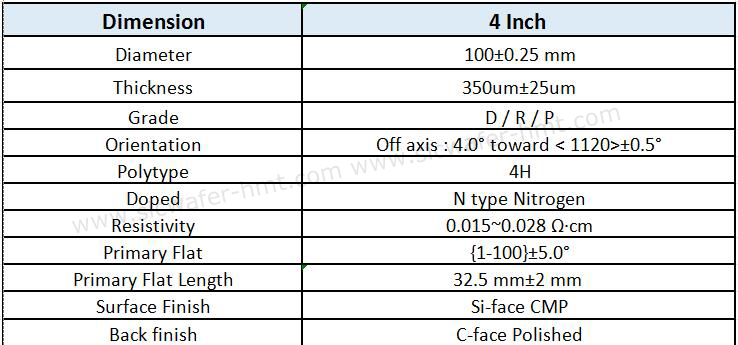
4 inch SiC Wafer Parameters
Applications of SiC Substrate Wafer
● Substrate wafer application: high-end lighting, SiC epitaxial wafer, GaN epitaxial wafer, PSS substrate, etc
● New energy vehicle applications: electric vehicle electric drive system power devices, charging pile power devices, etc
● Military applications: airborne radar communication equipment power devices, microwave communication high-power devices, etc
● Ultra-high speed integrated circuit: RFIC (Radio frequency integrated circuit), SOS chip, optical communication chip, 5G technology, etc
As the third generation of semiconductor materials, silicon carbide substrate has become one of the new semiconductor materials of great concern nowadays due to its excellent performance under high temperature, high pressure, high frequency and other conditions. The crystal structure of SiC silicon carbide determines its unique physical properties. Compared with Si and GaAs, SiC silicon carbide has better physical properties. The band gap is large, which is close to 3 times that of Si, ensuring the long-term reliability of the device under high temperature operation; The breakdown field strength is high, which is 10 times that of Si, ensuring the voltage tolerance of the device and improving the voltage tolerance of the device; The saturated electron rate is 2 times that of Si, which increases the operating frequency and power density of the device; High thermal conductivity, more than 3 times that of Si, increases the heat dissipation capacity of the device, and realizes the miniaturization of the device.
Related Products


![]() M.P: +86-15366208370 ; +86-15366203573
M.P: +86-15366208370 ; +86-15366203573
![]() E-mail: kim@homray-material.com ; tina@homray-material.com
E-mail: kim@homray-material.com ; tina@homray-material.com
HMT Gallium Nitride (GaN) Wafer Website: www.ganwafer-hmt.com