
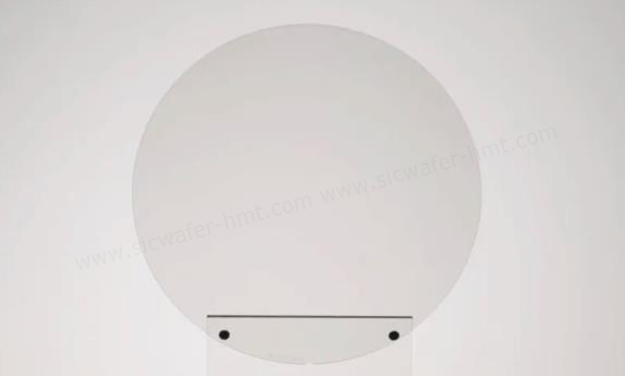
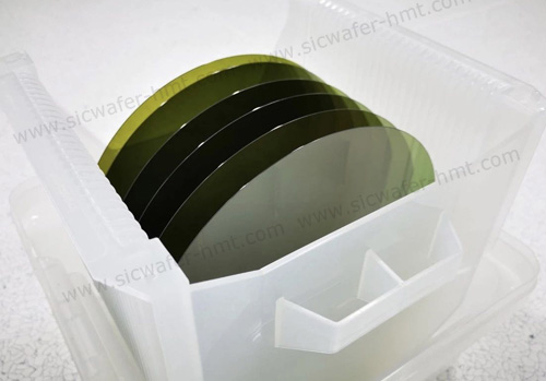
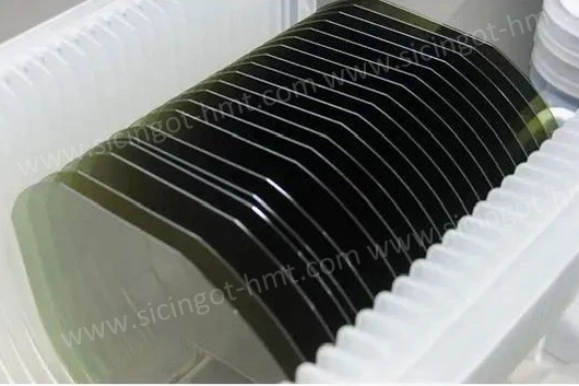
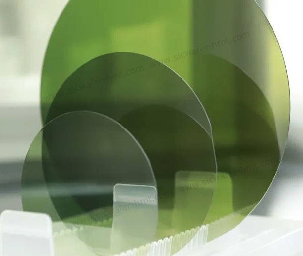
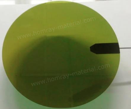
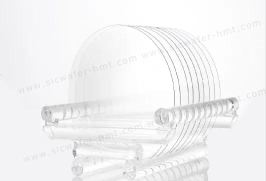
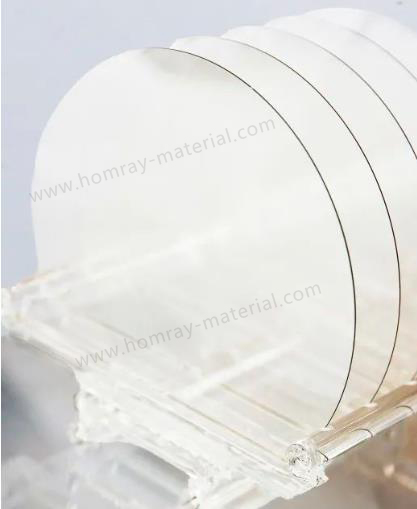
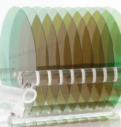
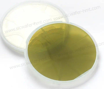
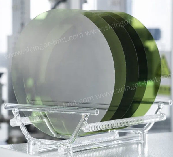
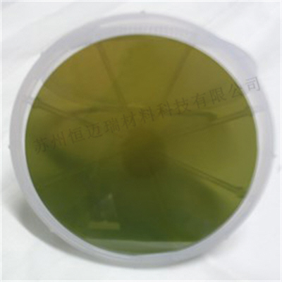
6 inch P Grade SiC Wafer Manufacturer
Type: 4H-N
Diameter: 6inch / 4inch
Grade: P Grade / D Grade
Product Name: SiC Substrate
Product Description
Buy high quanlity 6 inch SiC Wafer from HMT SiC substrate wafer manufacturer and supplier in China, we provide low cost but high quanlity P grade SiC Wafer with 4H-N type and 4H-SI type. Our SiC wafers have been widely used by small and large semiconductor poewer device companies as well as research labs/high schools worldwide.Custom-made epitaxial wafers such as SiC-on-SiC and GaN-on-SiC wafers are also available from HMT company.
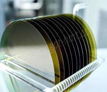
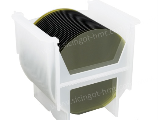
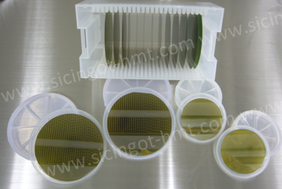
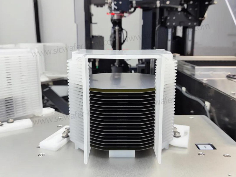
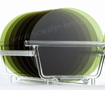
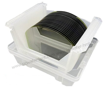
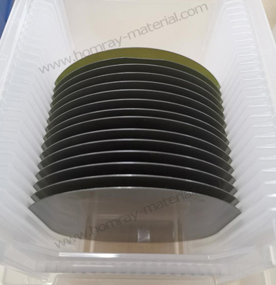
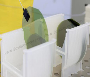
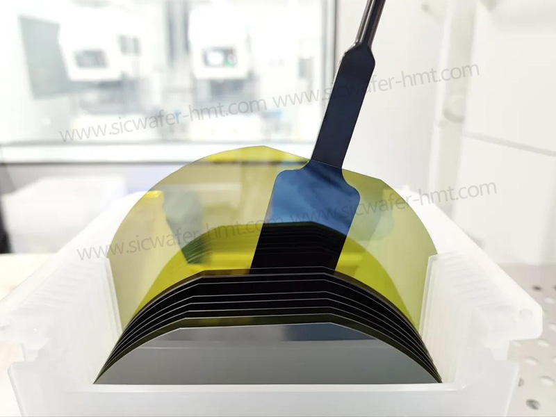
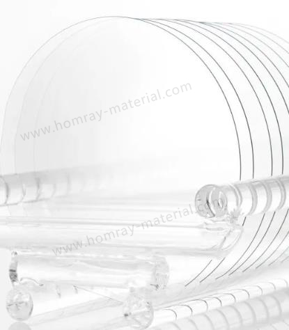
We use Cassette to package SiC Wafers and wafer box to package SiC Boules.
At present, SiC powder is mainly synthesized from high purity carbon powder and silicon powder, using physical vapor transfer method (PVT method), growing into crystals in a single crystal furnace, and then SiC crystal through slicing, grinding, polishing, cleaning and other steps to make a single crystal sheet as the substrate.
There are two major difficulties in the preparation of SiC crystal, one is that the growth rate of SiC crystal rod is slow, and the growth time of about 2cm crystal rod is 7-10 days; Second, SiC crystal growth has high requirements for various parameters, requiring precise control of silicon-carbon ratio, growth temperature gradient and other parameters, and the growth process is difficult to monitor, and the process requirements are very high.
Related Products


![]() M.P: +86-15366208370 ; +86-15366203573
M.P: +86-15366208370 ; +86-15366203573
![]() E-mail: kim@homray-material.com ; tina@homray-material.com
E-mail: kim@homray-material.com ; tina@homray-material.com
HMT Gallium Nitride (GaN) Wafer Website: www.ganwafer-hmt.com