
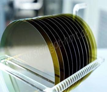
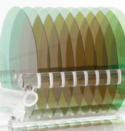
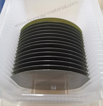
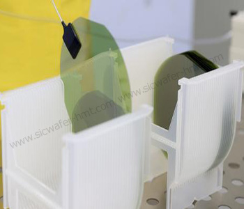
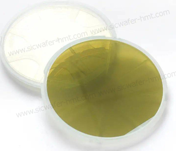
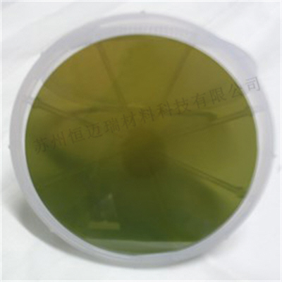
4 inch P Grade SiC Substrate Manufacturer SiC VS Silicon Advantages
Grade: D/R/P Grade
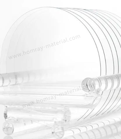
Type: 4H-HPSI/4H-N
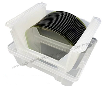
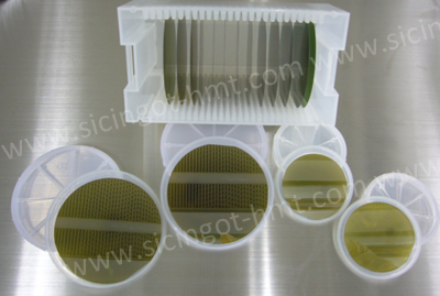
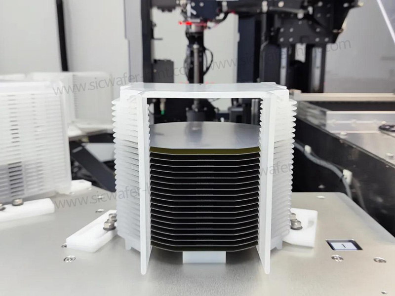
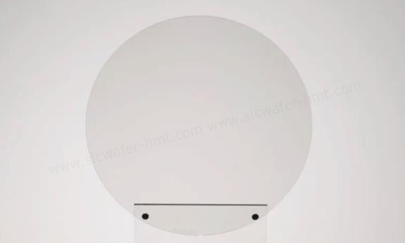
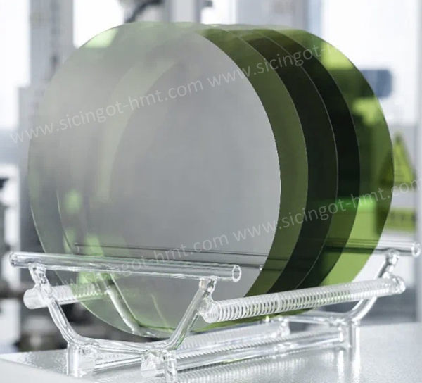
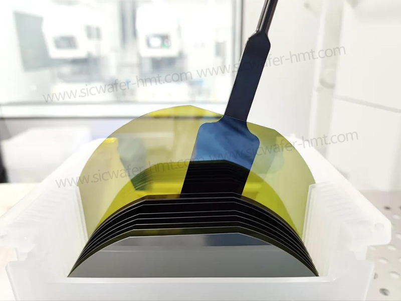
Dimension:2inch 4inch 6inch 8inch
Thickness:350±25um/500±25um
Product Description
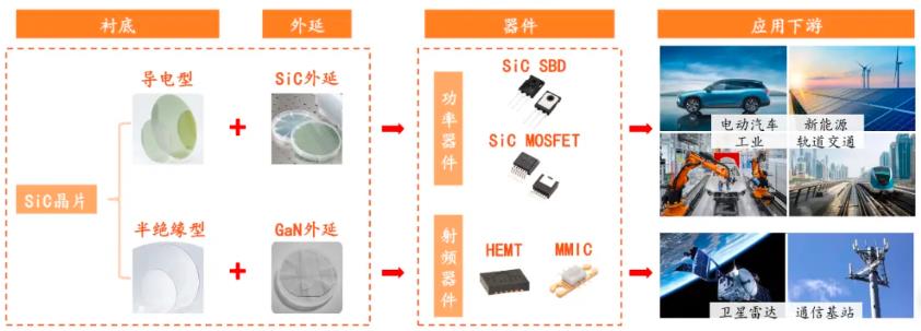
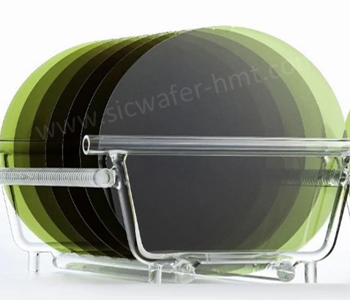
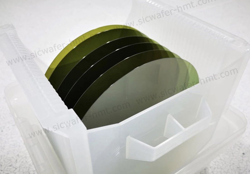
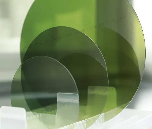
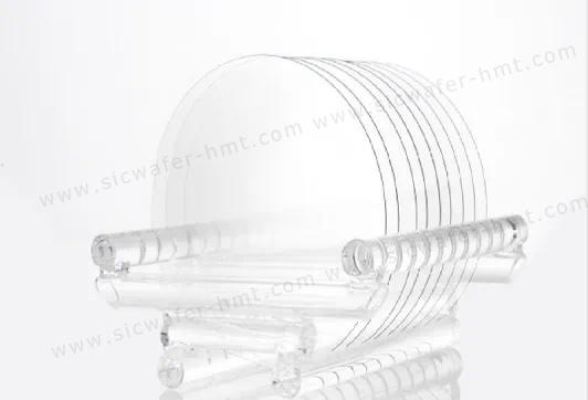
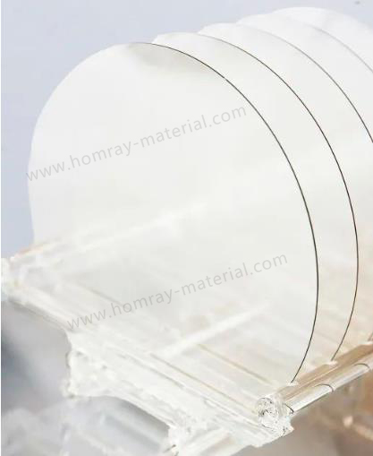
Silicon carbide (SiC) substrates are divided into semi-insulating SiC substrates, which refer to substrates with a resistivity higher than 1E5ohm·cm. HMT offers 4inch to 8inch SI type SiC Wafers with Dummy grade and Production Grade. These are primarily used in the manufacturing of GaN microwave radio frequency (RF) devices. Microwave RF devices are fundamental components in the field of wireless communication, and the vigorous development of 5G communication technology in China has further driven the demand for SiC substrates.
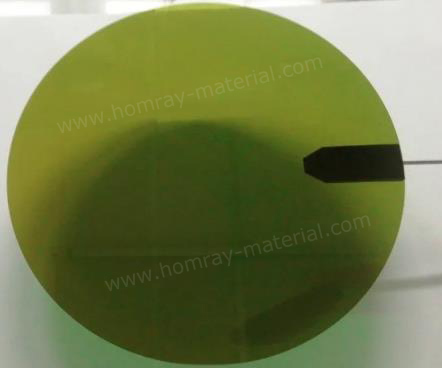
On the other hand we also offers Conductive N type SiC substrates from 2inch to 8inch which have a resistivity ranging from 0.015-0.025ohm.cm. The epitaxial wafers grown from conductive SiC substrates can be further processed into power devices, which are core components in power electronic conversion systems. These power devices are widely used in new energy vehicles, photovoltaic systems, smart grids, rail transportation, and other fields.
SiC MOSFETs or SiC FETs offer several advantages compared to silicon-based devices. The higher breakdown voltage of SiC allows for thinner and lighter devices that can support higher voltages. Other advantages of SiC over silicon include:
- As a wide bandgap material, it exhibits lower leakage currents under high-temperature conditions.
- Higher thermal conductivity, which supports high current density applications.
- Lower energy losses, helping to minimize power dissipation.
- Higher switching frequencies, which reduce the size and weight of large peripheral passive components.
- Smaller die size and lower parasitic capacitance result in lower switching losses, enabling power converters to operate at higher switching frequencies and speeds.
- Ability to function at higher ambient temperatures, which helps reduce the size of heat sinks.

Related Products


![]() M.P: +86-15366208370 ; +86-15366203573
M.P: +86-15366208370 ; +86-15366203573
![]() E-mail: kim@homray-material.com ; tina@homray-material.com
E-mail: kim@homray-material.com ; tina@homray-material.com
HMT Gallium Nitride (GaN) Wafer Website: www.ganwafer-hmt.com