
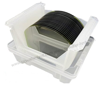
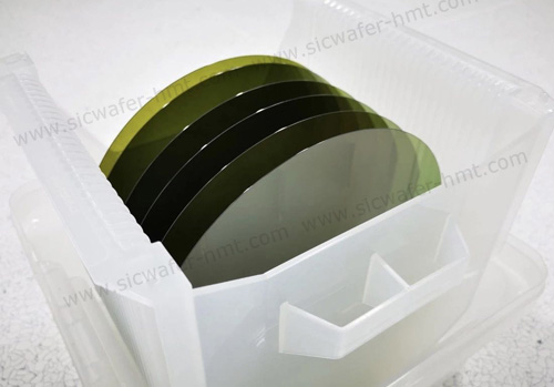
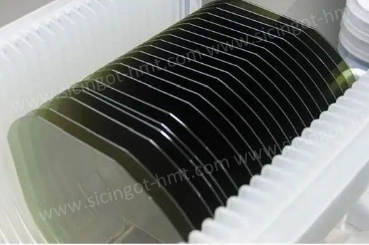
HPSI 8 Inch SiC Substrate Wafer Manufacturer
Type:HPSI
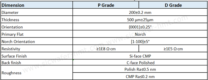
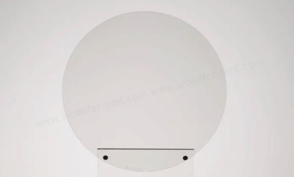
Diameter: 200±0.2mm
Thickness: 500±25um
Grade: D and P
Product Description
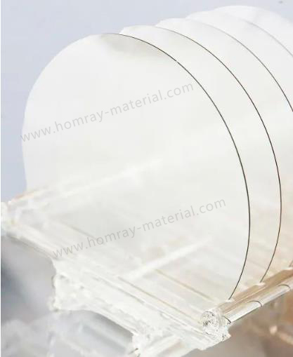
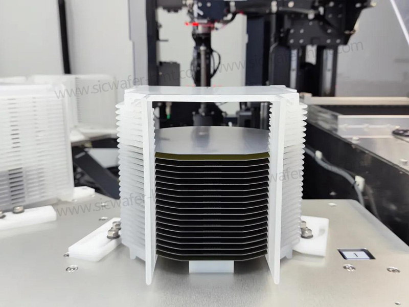
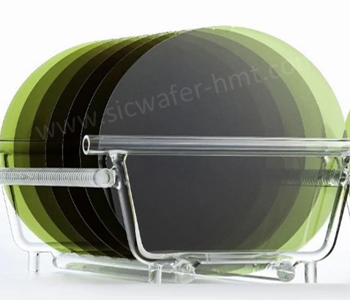
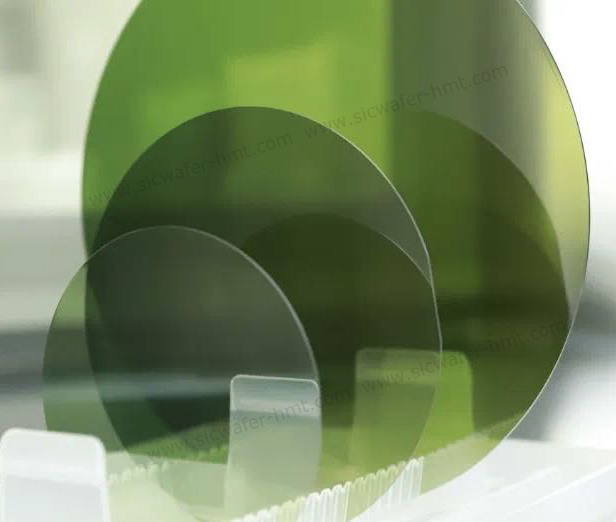
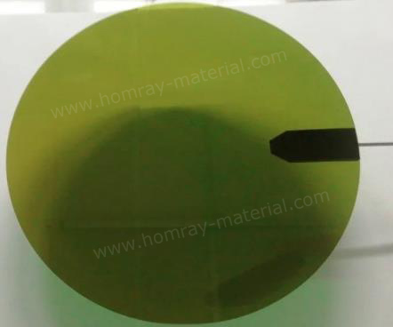
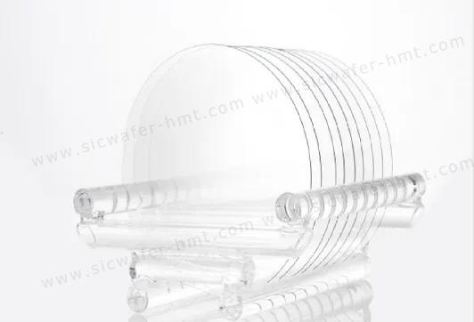
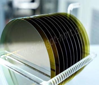
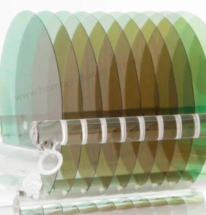
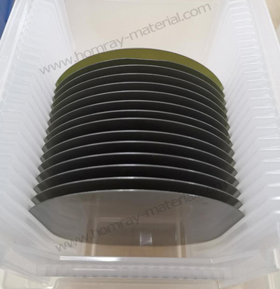
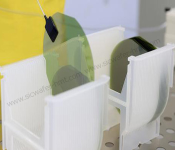
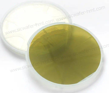
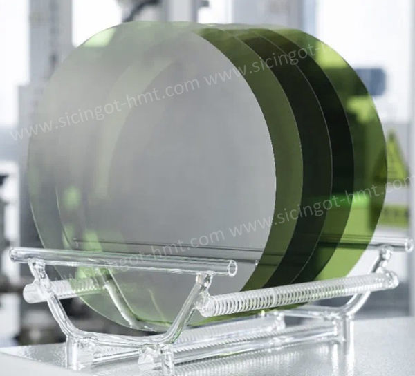
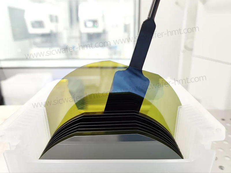
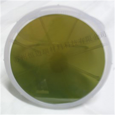
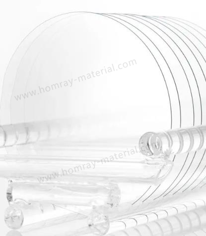
HMT as the professional SiC Boule and SiC substrate wafer manufacturer, we can produce diameter 200mm 8 inch Semi-insualted SiC Substrate wafer. Actually, 8 inch is the most newest and biggest dimension of SiC products on the market. Not only Conductive N type, but also Semi-insulating type both are available in HMT. We provide D grade 8 inch SiC substrate and P grade SiC substrate for different applications.
8 inch basic parameters. Please contact us for more detailed technical data.
SiC substrates can be divided into semi-insulating and conductive types. The semi-insulated substrate mainly achieves the intrinsic high resistivity of the crystal by removing various impurities in the crystal (especially shallow level impurities), while the conductive substrate achieves the low crystal resistivity by introducing nitrogen in the crystal growth process.Semi-insulated SiC substrate: suitable for high frequency, high temperature and other working environments, mainly used in 5G, radar and other fields.
Related Products


![]() M.P: +86-15366208370 ; +86-15366203573
M.P: +86-15366208370 ; +86-15366203573
![]() E-mail: kim@homray-material.com ; tina@homray-material.com
E-mail: kim@homray-material.com ; tina@homray-material.com
HMT Gallium Nitride (GaN) Wafer Website: www.ganwafer-hmt.com