
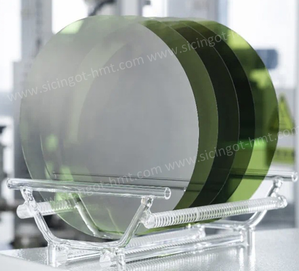
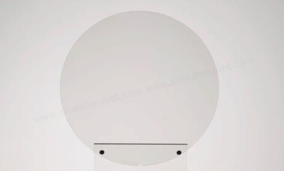
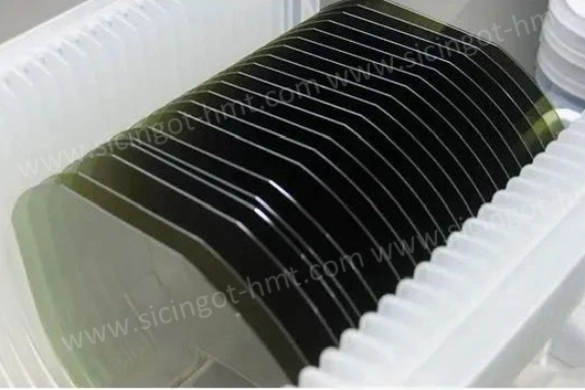
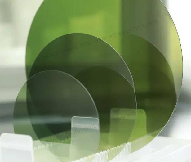
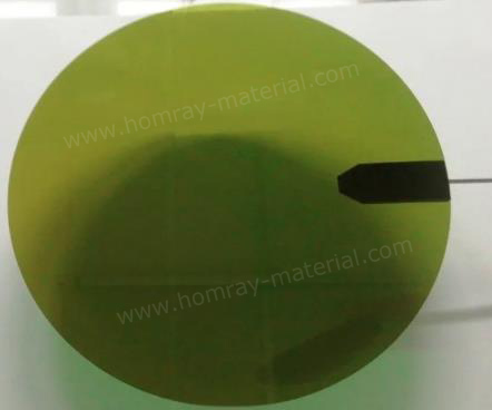
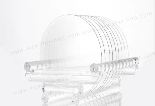
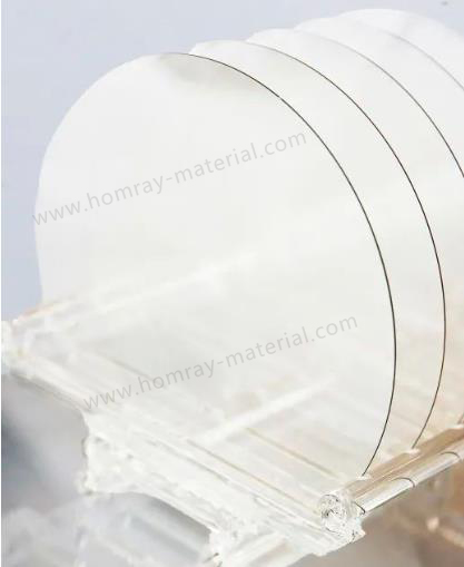
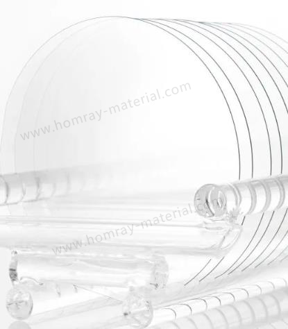
Conductive 4H-N 6 Inch SiC Substrate Manufacturer
Dimension:6inch
Grade: Dummy Grade
Type: 4H-N
Thickness: 350um
Product Description
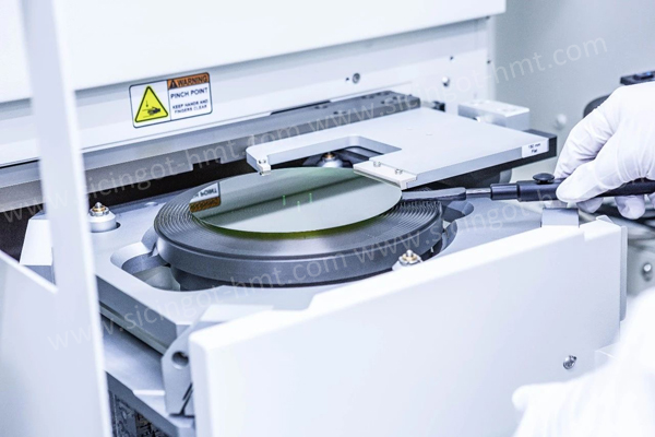
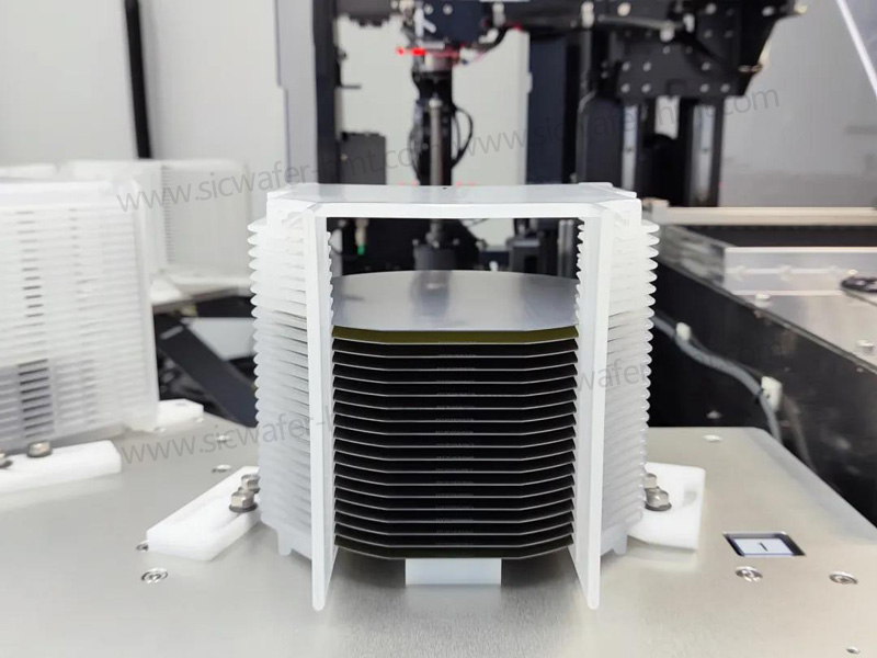
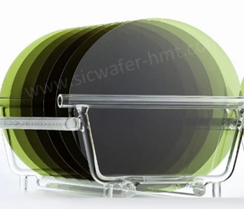
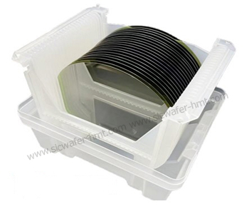
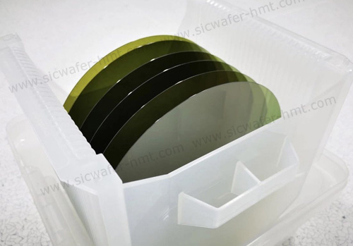
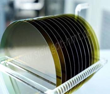
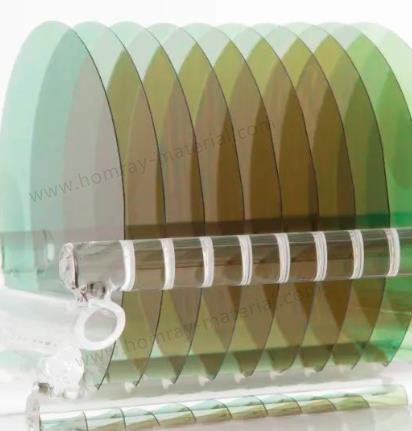
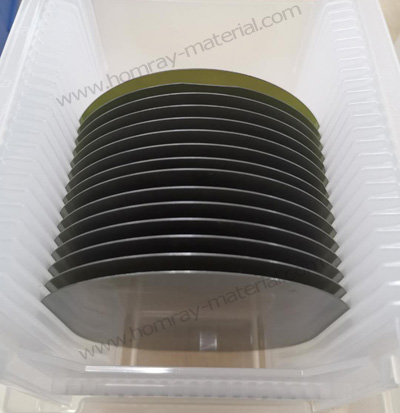
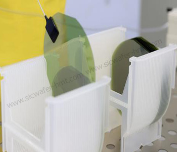
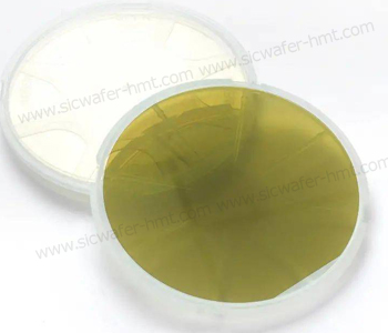
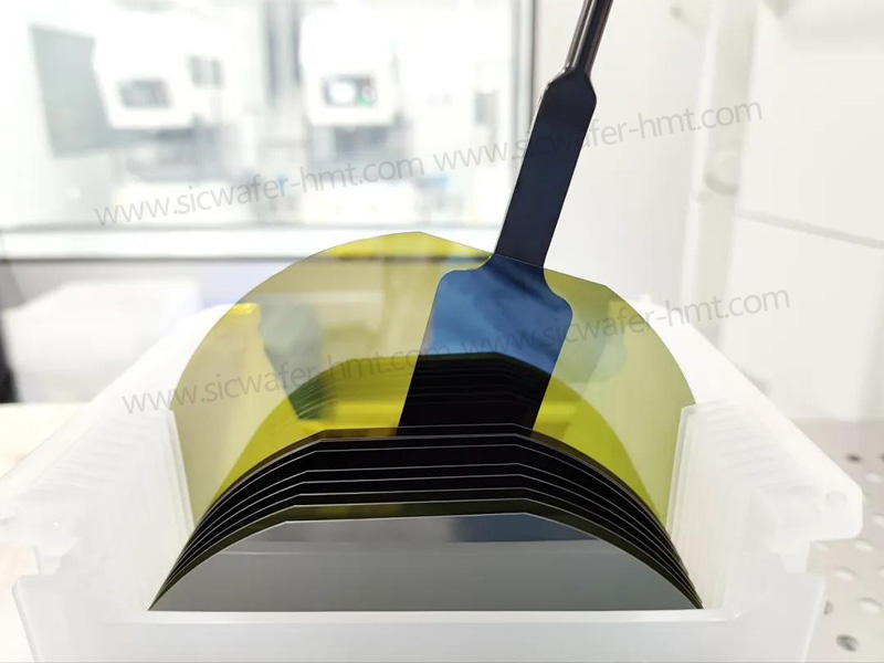
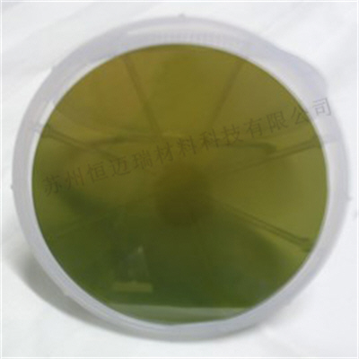
As the professional 6 inch SiC Wafer Manufacturer, HMT company supply Dummy Grade and Production Grade 6 inch SiC Substrate Wafer with very competitive price on the SiC market. We can supply both 4H-N type and 4H-HPSI type with high quanlity low MPD. The normal thickness of 6 inch SiC wafer is 350um, but we can also supply 500um thickness. Conductive N type SiC Substrats can be used for SiC on SiC epi wafer, SBD, MOSFET etc power devices.

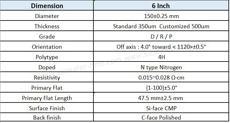
6 inch SiC Substate Basic Parameters
Semi-insulating SiC substrates are mainly used in gallium nitride rf devices. By growing gan epitaxy layer on semi-insulating SiC substrate, SiC based GAN epitaxy sheet can be further made into GAN radio frequency device. Microwave radio frequency components is the foundation of realize the signal sending and receiving components, is the core of the wireless communication, mainly including rf switch, LNA, power amplifier, filter and other devices, among them, the power amplifier is rf signal amplification device, directly determine the mobile terminal and base station of wireless communication distance, key parameters such as the signal quality.
Conductive SiC substrate: refers to the resistivity of SiC substrate in 0.015-0.028ohm.cm. SiC epitaxial wafers grown from conductive SiC substrates can be further made into power devices. Power devices are the core components of power electronics conversion devices, which are widely used in new energy vehicles, photovoltaic, smart power grids, rail transit and other fields. Automotive electrification trend is favorable for SiC development.
Related Products


![]() M.P: +86-15366208370 ; +86-15366203573
M.P: +86-15366208370 ; +86-15366203573
![]() E-mail: kim@homray-material.com ; tina@homray-material.com
E-mail: kim@homray-material.com ; tina@homray-material.com
HMT Gallium Nitride (GaN) Wafer Website: www.ganwafer-hmt.com