

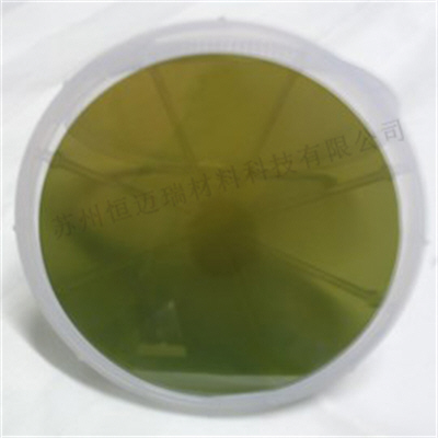
Custom 4H-N 800um SiC Substrate Manufacturer
Grade: D/R/P Grade
Type: 4H-N
Dimension: 6inch
Thickness:500±25um/800±25um
Product Description
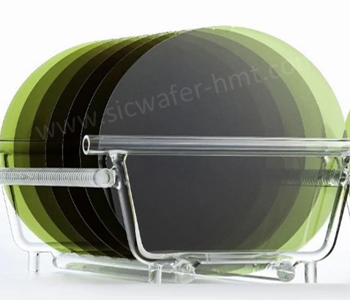
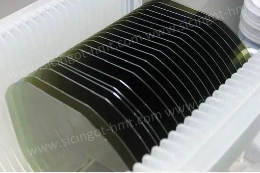
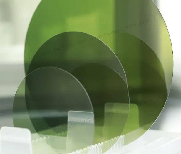
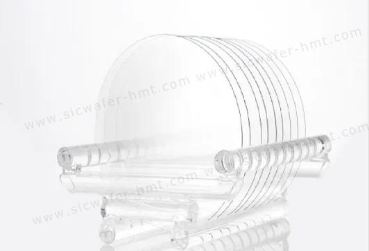
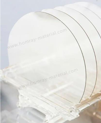
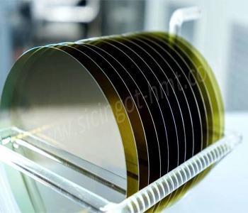
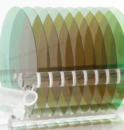
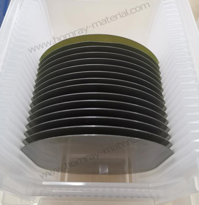
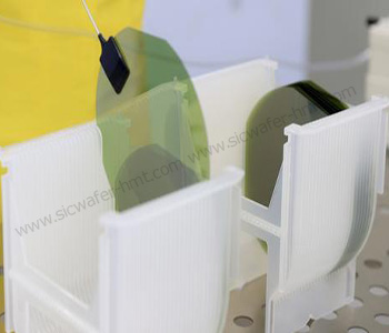
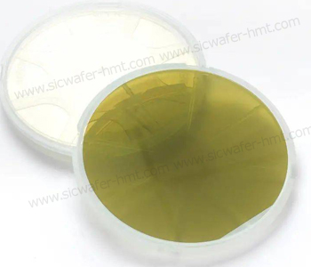
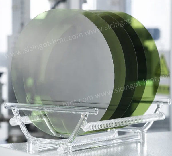
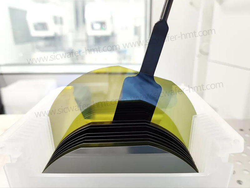
As a leading Silicon Carbide (SiC) substrate manufacturer in China, we specialize in high-performance custom SiC wafers, including industry-leading 800µm thickness on 6-inch substrates. While standard 4H-N type SiC wafers typically measure 350µm, we excel in producing 500µm and 800µm variants tailored for high-power, high-voltage devices requiring exceptional mechanical stability and thermal performance.
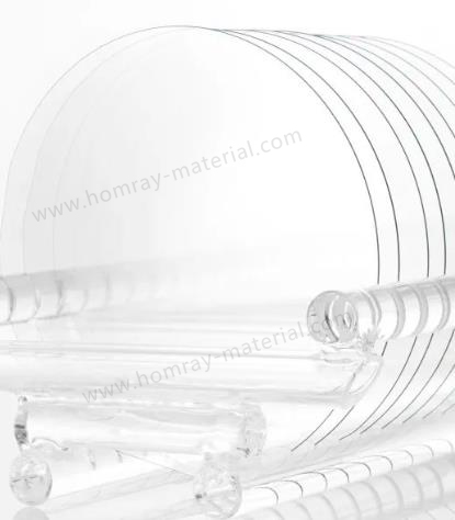
All our substrates undergo precision double-side polishing, achieving an outstanding surface roughness of Ra < 0.5 nm. This ensures superior epitaxial layer quality and device yield. We deliver both standard specifications and custom-engineered solutions to meet your project's exact requirements for thickness, diameter, and polytype.

-
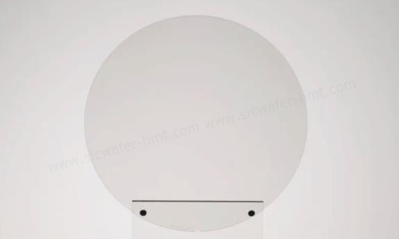
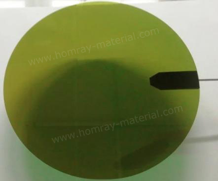
Size: 6inch;
-
Diameter: 150mm±0.25;
-
Thickness: 800um±25;
-
Surface Orientation: 4°toward[11-20]±0.5°;
-
Primary Flat orientation:[1-100]±5°;
-
Primary Flat Length:47.5mm±1.5;
-
Secondary flat: None;
-
Micropipe: ≤0.2/cm2;
-
Resistivity: 0.015~0.028Ω;
-
TTV≤10um;
-
Warp≤35um;
-
Bow≤35um;
-
Surface Roughness: Si face Ra<0.5 nm;
-
Surface finish: Double Side Polish, Si Face CMP;
-
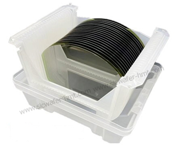
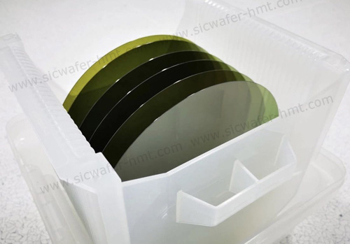
Packing: Multi-wafer Cassette Or Single Wafer Container;
Partner with us for reliable, high-purity SiC substrates that push the boundaries of power electronics, RF devices, and advanced semiconductor applications. Contact us Now!
Related Products


![]() M.P: +86-15366208370 ; +86-15366203573
M.P: +86-15366208370 ; +86-15366203573
![]() E-mail: kim@homray-material.com ; tina@homray-material.com
E-mail: kim@homray-material.com ; tina@homray-material.com
HMT Gallium Nitride (GaN) Wafer Website: www.ganwafer-hmt.com