
AR Lenses HPSI SiC Substrate Manufacturer
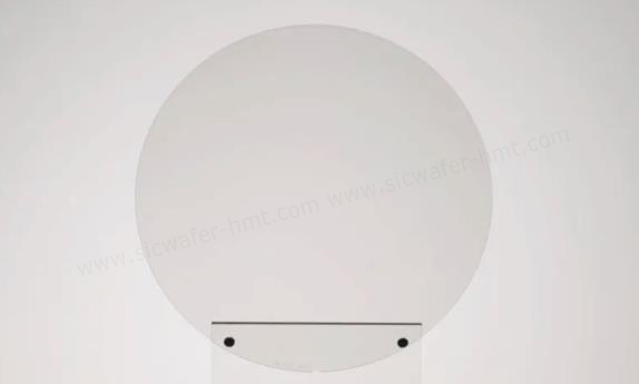
Grade: D/P Grade
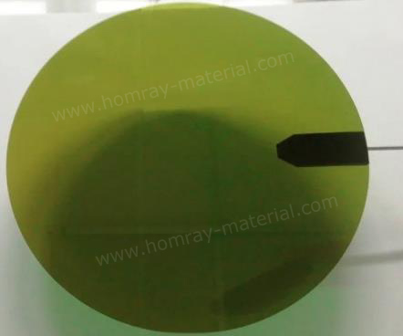
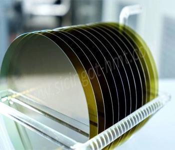
Type: 4H-HPSI
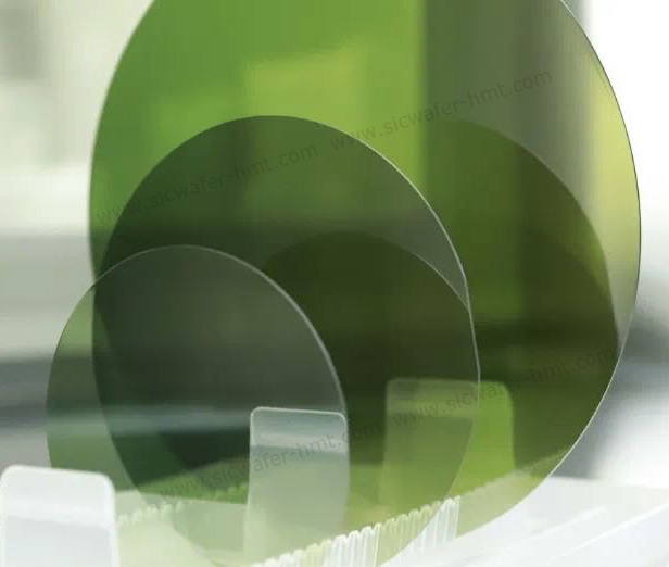
Dimension:4inch 6inch 8inch
Thickness:500±25um
Product Description
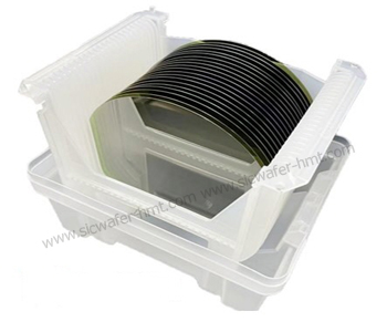
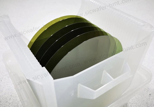
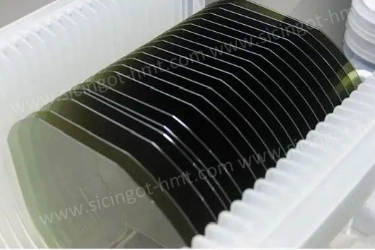
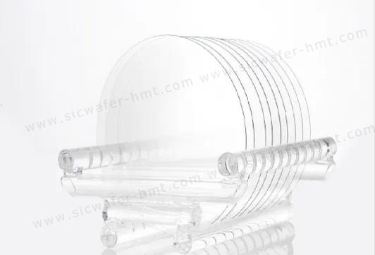
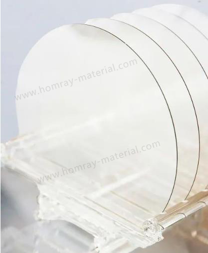
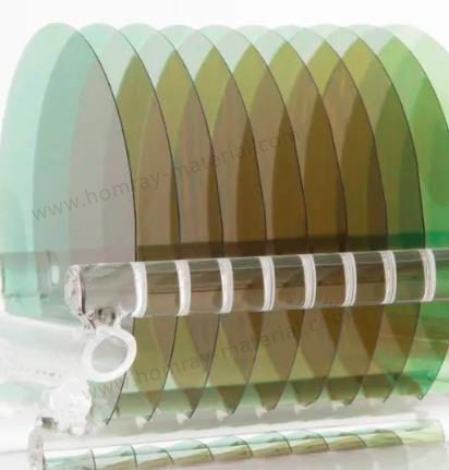
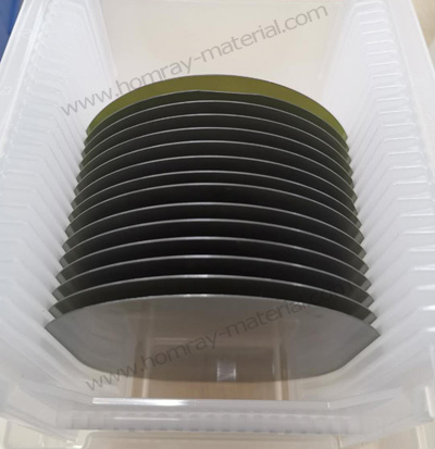
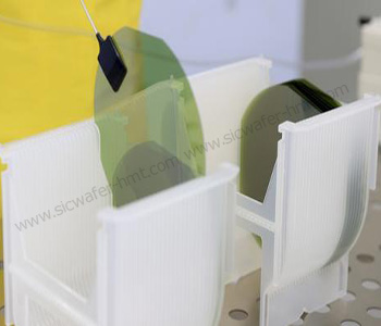
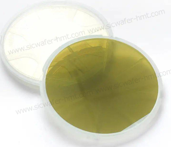
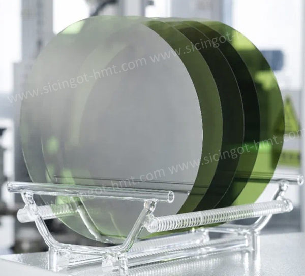
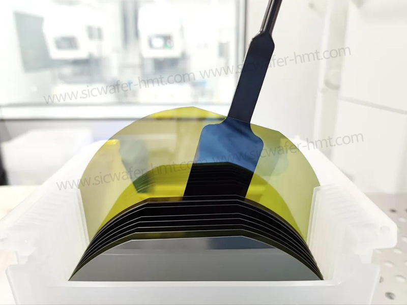
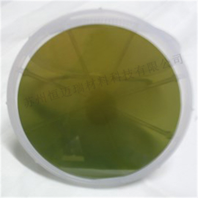
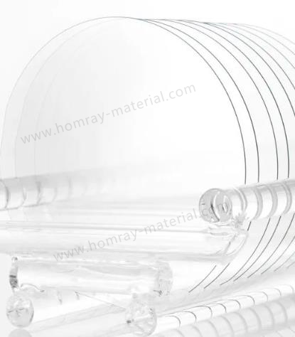
In recent years, silicon carbide (SiC) has emerged as a groundbreaking material, leveraging its exceptional physical and optical properties to become widely used in various power semiconductor devices and modules. Now, it is also crossing over to become a critical material in the field of AR glasses. HMT company as the leading SiC Substrate Wafer Manufacturer always produces 100mm4inch 150mm6inch and 200mm8inch high quanlity HPSI type SiC Substrate for AR lenses, AR newest technologies.
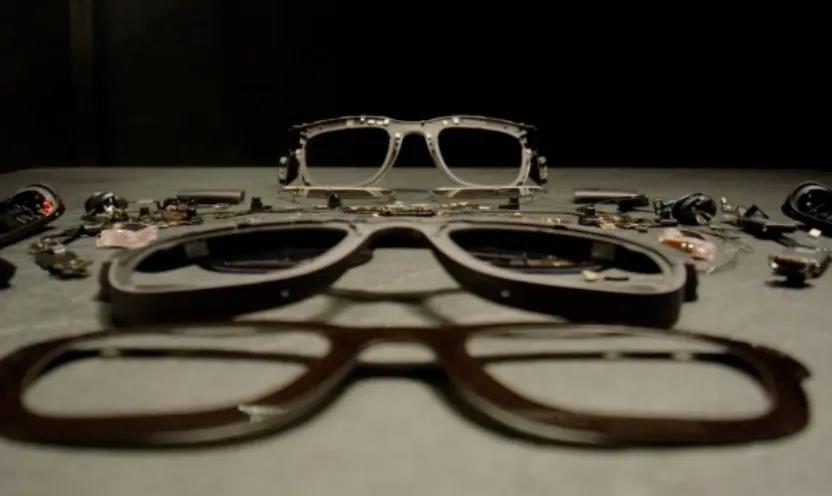
The high refractive index, superior thermal conductivity, and high hardness of SiC demonstrate significant potential in enhancing the display technology, lightweighting, and thermal management of AR glasses.
The advantages of SiC are primarily reflected in the following aspects:
1. High Refractive Index: SiC boasts a refractive index of over 2.6, far exceeding that of traditional materials like resin (1.51-1.74) and glass (1.5-1.9). A high refractive index means SiC can more effectively confine light propagation, reducing optical energy loss and thereby improving display brightness and field of view (FOV). For instance, Meta's Orion AR glasses, utilizing SiC waveguide technology, achieve a 70-degree FOV, significantly surpassing the 40-degree FOV of traditional glass materials.
2. Exceptional Thermal Performance: The thermal conductivity of SiC is hundreds of times greater than that of ordinary glass, enabling rapid heat dissipation. For AR glasses, thermal management is a critical issue, especially during high-brightness displays and prolonged usage. SiC lenses can quickly dissipate heat from the optical engine, enhancing device stability and lifespan.
3. High Hardness and Wear Resistance: SiC is one of the hardest known materials, second only to diamond. This makes SiC lenses highly wear-resistant and suitable for everyday use. In contrast, glass and resin materials are prone to scratches, negatively impacting user experience.
Related Products


![]() M.P: +86-15366208370 ; +86-15366203573
M.P: +86-15366208370 ; +86-15366203573
![]() E-mail: kim@homray-material.com ; tina@homray-material.com
E-mail: kim@homray-material.com ; tina@homray-material.com
HMT Gallium Nitride (GaN) Wafer Website: www.ganwafer-hmt.com