

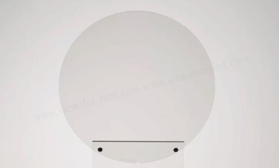
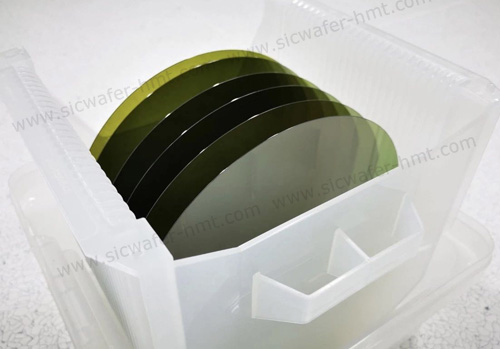
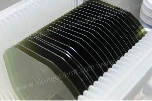
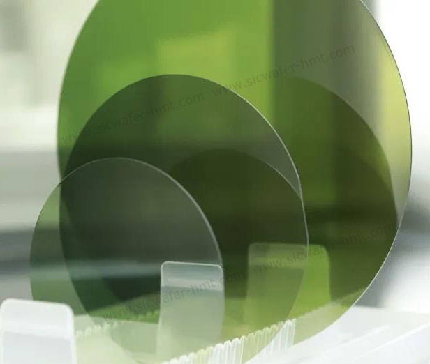
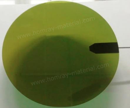
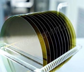
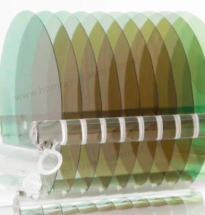
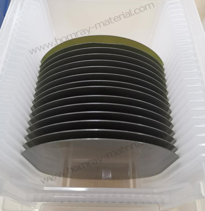
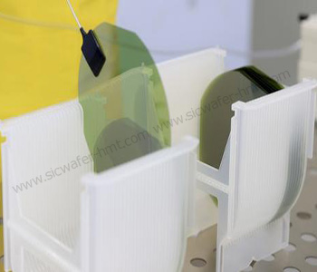
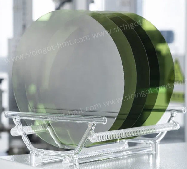
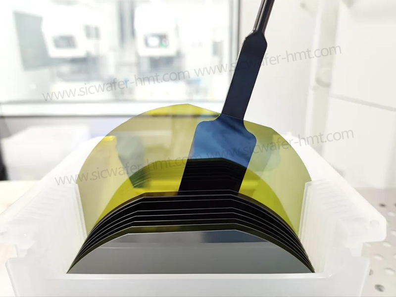
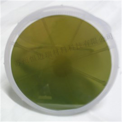
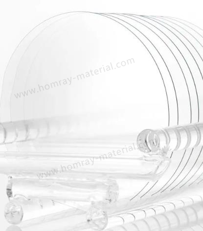
2 inch SiC Wafer Manufacturer
Product Name: SiC Substrate
Grade: Dummy Grade
Type: 4H-N
Dimension: 2 inch
Product Description
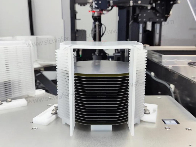
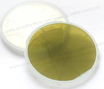
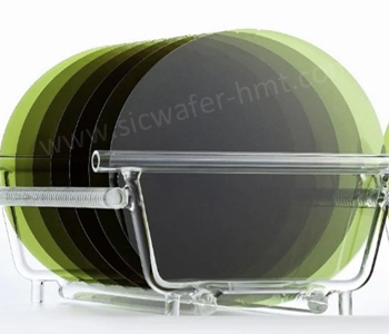
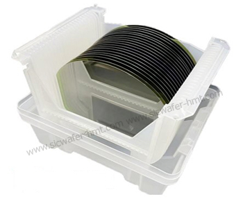
Are you looking for 2 inch SiC Substrate Wafer Manufacturer? HMT providing 50.8mm 2 inch SiC Substrate wafer with Conductive N type only. Actually, 2 inch SiC Wafer is stop production many years for most factories, the mainstream is 6 inch and 8 inch SiC substrate wafers. But HMT company still keep few capacity allocation for 2 inch SiC Wafers 2 inch Boules for some customers.If you have 2 inch SiC Products purchase demand now, contact HMT company immediately and let us know your requirements.
SiC wafer Application

2 inch SiC Wafer
 SiC has wide band gap width, high breakdown electric field, high thermal conductivity and high electron saturation rate of physical properties, so that it has high temperature resistance, high pressure resistance, high frequency, high power, radiation resistance and other advantages, can reduce downstream product energy consumption, reduce terminal volume. The band gap width of SiC is about 3.2eV, and the wide band width of silicon is 1.12eV, which is about 1/3 of the band gap width of SiC, indicating that SiC has significantly better high pressure resistance than silicon material.
SiC has high energy conversion efficiency, and will not decrease with the increase of frequency, SiC device operating frequency can reach 10 times of silicon based devices, the same specification of SiC MOSFET total energy loss is only 30% of silicon based IGBT.
SiC materials will gradually replace silicon in the fields of high temperature, high frequency and high frequency, and play an important role in 5G communications, aerospace, new energy vehicles and smart power grids.
Related Products


![]() M.P: +86-15366208370 ; +86-15366203573
M.P: +86-15366208370 ; +86-15366203573
![]() E-mail: kim@homray-material.com ; tina@homray-material.com
E-mail: kim@homray-material.com ; tina@homray-material.com
HMT Gallium Nitride (GaN) Wafer Website: www.ganwafer-hmt.com