
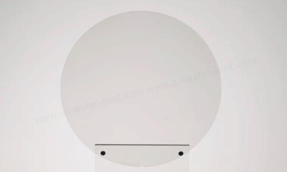
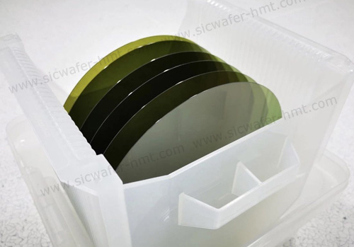
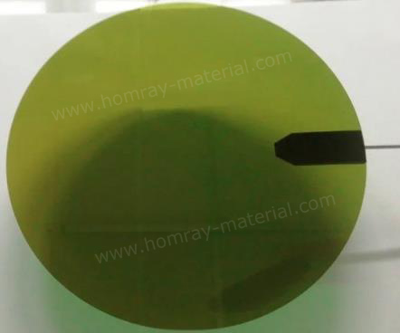
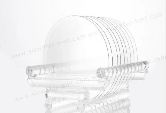
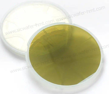
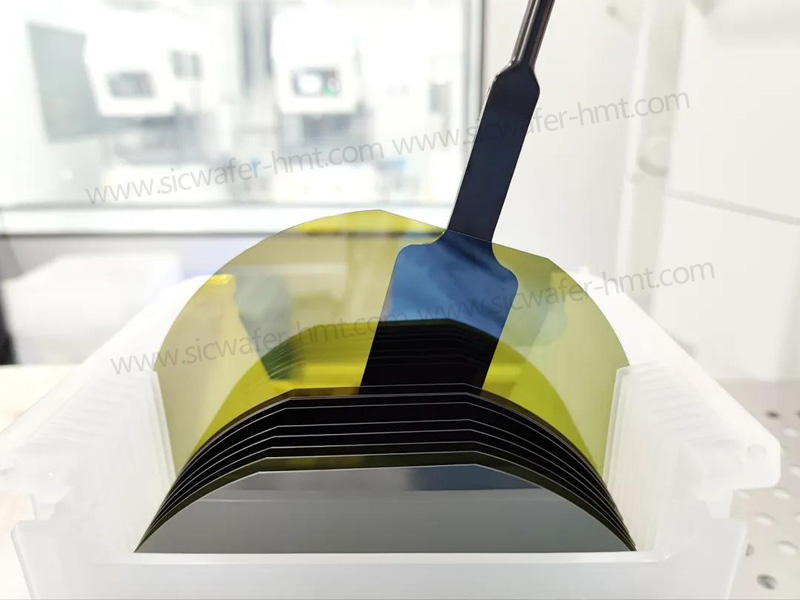
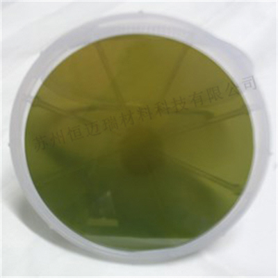
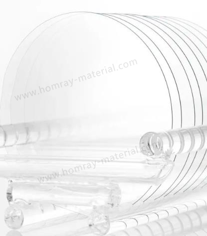
P Grade 6 inch 4H-HPSI SiC Wafer AR AI
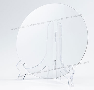
Dimension:6 Inch
Grade: Production Grade
Type: 4H-HPSI
Thickness: 500um
Product Description
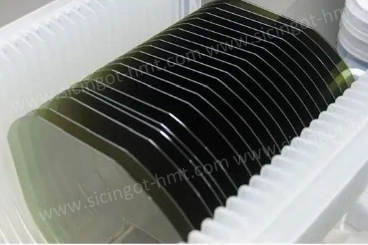
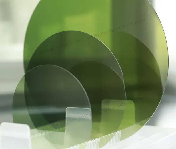
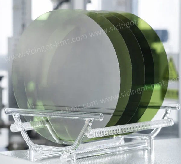
As a premier global manufacturer of 4H-SiC wafers, HMT is pioneering the future of AR and AI with our specialized Optical AR/AI Silicon Carbide SiC Wafers. Available in both 6 inch and 8 inch dimensions, these wafers are engineered to meet the extreme demands of next-generation optical systems.
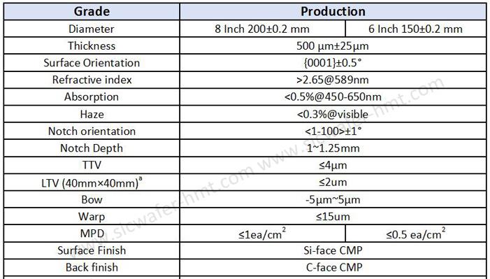
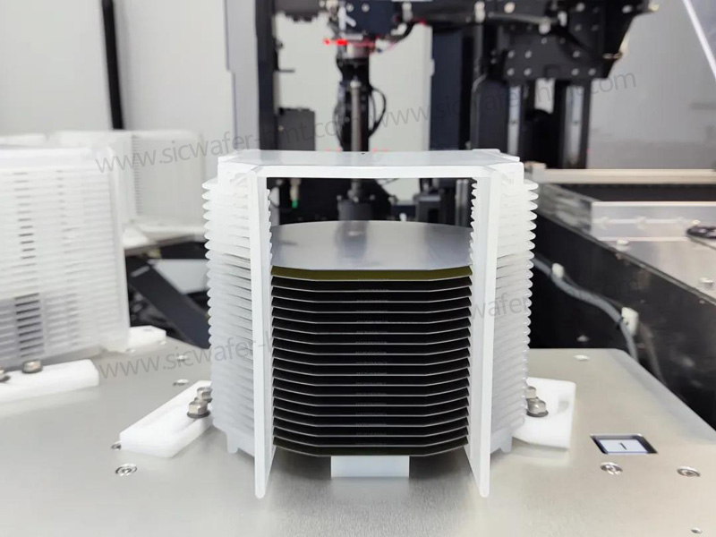
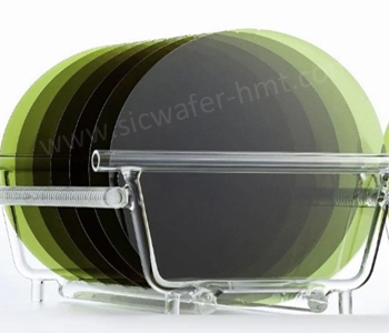
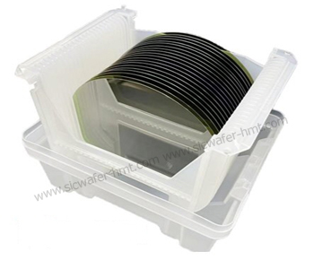
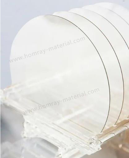
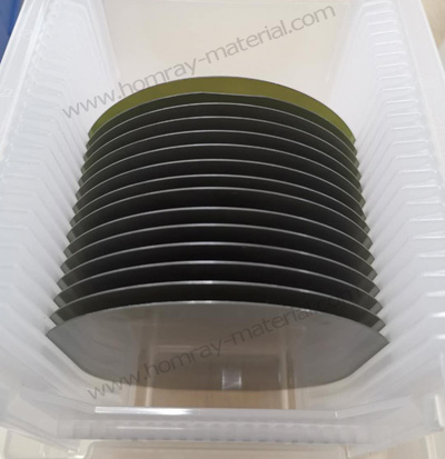
Our High-Purity Semi-Insulating (HPSI) SiC wafers feature a standard thickness of 500µm and are meticulously double-side polished to achieve an ultra-smooth surface, which is critical for high-fidelity nanoscale lithography.
In physical properties
SiC is known as the "optical diamond," second only to diamond in hardness. This exceptional hardness ensures that it maintains structural stability and precision in nanoscale etching processes, meeting the stringent requirements of AR waveguides for grating period (which must be accurate to the nanoscale) and etching depth (with errors less than 5 nm). This effectively prevents issues such as rainbow patterns and optical efficiency attenuation caused by material deformation or machining inaccuracies.
In optical performance
Silicon carbide boasts an extremely high refractive index (approximately 2.6-2.8) and outstanding light transmittance, enabling efficient reflection and transmission of light at specific wavelengths (such as the visible light spectrum commonly used in AR devices). This characteristic makes it an ideal material for optical waveguides. As the "optical backbone" of AR glasses, waveguides need to efficiently transmit image light from micro-displays to the human eye while allowing ambient light to pass through normally (to avoid obstructing the view). The high refractive index of silicon carbide, combined with precisely designed grating structures, enables total internal reflection confinement and directional coupling of light, reducing optical losses during transmission and resulting in brighter and clearer AR imagery.
Additionally, silicon carbide's high-temperature resistance and strong chemical stability allow it to adapt to various environmental conditions in which AR glasses are used (such as high-temperature outdoor settings or humid environments). It also demonstrates superior compatibility with other materials (such as photoresists and metal coatings), facilitating the large-scale mass production of waveguide components.
Related Products


![]() E-mail: kim@homray-material.com ; tina@homray-material.com
E-mail: kim@homray-material.com ; tina@homray-material.com
HMT Gallium Nitride (GaN) Wafer Website: www.ganwafer-hmt.com