
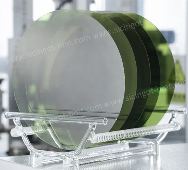
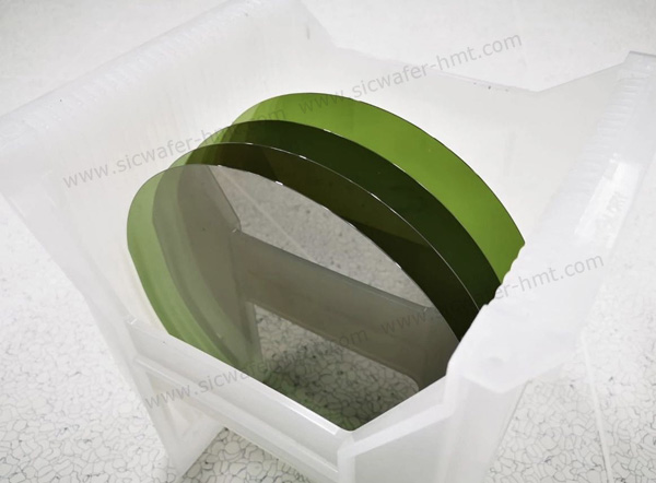
P Grade 8 inch SiC Wafer Manufacturer
Type: 4H-N
Diameter:200mm
Grade: Production
Product Name: SiC Wafer
Product Description
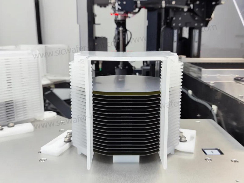
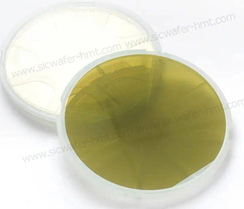
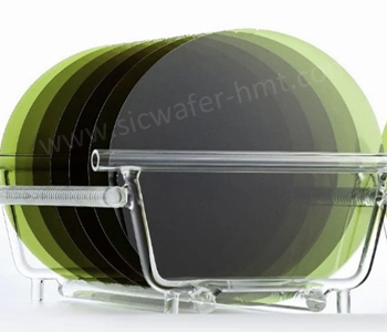
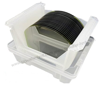
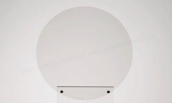
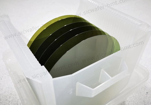
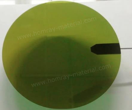
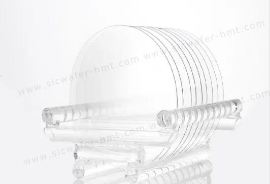
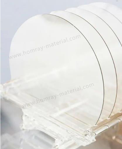
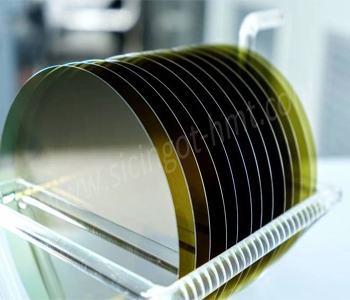
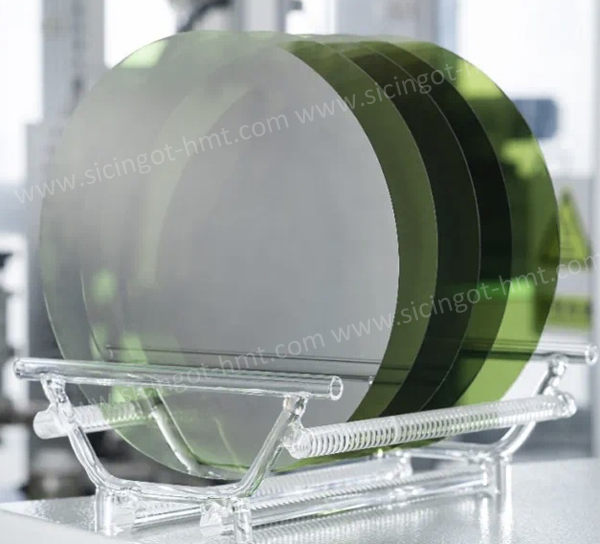
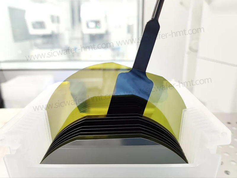
8 Inch P Grade 4H-N SiC Wafer
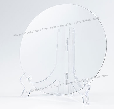
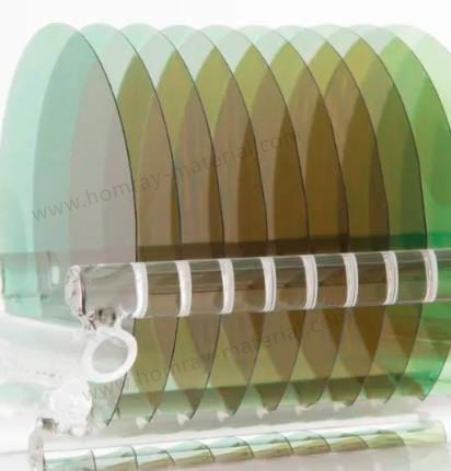
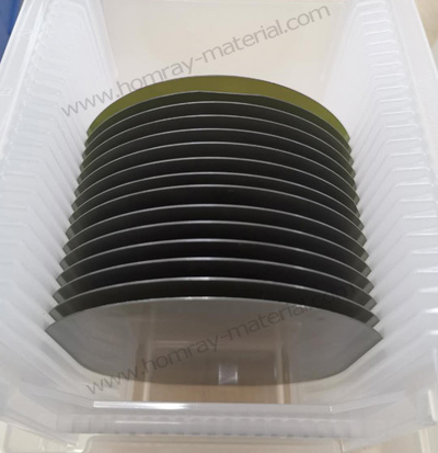
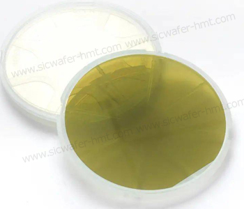
HMT provides 8 inch P Grade 4H-N SiC wafers with a 200 mm diameter for production-oriented semiconductor development and SiC device fabrication. The current standard specification is 500 μm ±25 μm thickness with 0.01–0.028 Ω·cm resistivity, with other wafer parameters available according to application requirements.
8 Inch P Grade SiC Wafer Specifications
The wafer diameter is 200 mm (8 inch) and the crystal structure is 4H-SiC, with the current product configured as N-type production-grade material. The standard thickness is 500 μm ±25 μm, while the specified resistivity range is 0.01–0.03 Ω·cm.
| Parameter | Technical Specification |
| Diameter | 200mm ± 0.2mm (8 inch) |
| Polytype & Type | 4H-N Conductive |
| Resistivity | 0.01 – 0.03 Ω·cm |
| Thickness | 500μm ± 25μm |
| Surface Roughness (Ra) | < 0.2 nm (CMP Polished) |
What Is an 8 Inch P Grade SiC Wafer?
An 8 inch P Grade SiC wafer is a 200 mm production-grade 4H-SiC substrate designed for applications that require a larger wafer format than 4 inch or 6 inch substrates. The 200 mm diameter provides approximately 78.5% more wafer surface area than a 150 mm wafer, allowing more device structures to be processed on each wafer.
The P Grade designation identifies the product as a production-oriented wafer grade, rather than a dummy or purely research-grade substrate. For customers developing power semiconductor processes, the grade should be evaluated together with resistivity, defect specifications, surface quality and geometry requirements.
Production Grade vs Dummy Grade SiC Wafer
Production-grade SiC wafers are intended for customers who need a substrate closer to device-processing requirements, while dummy-grade wafers are generally selected for equipment qualification, process trials or non-device testing. The key distinction is not simply wafer diameter but the required combination of material quality, geometry, surface condition and defect specifications.
For process qualification, a lower-cost dummy substrate may be sufficient; for device-related development, a production-grade substrate is normally the more relevant starting point. HMT also supplies different SiC wafer grades so customers can select the substrate according to process stage and budget.
8 Inch SiC Wafer Manufacturing Process
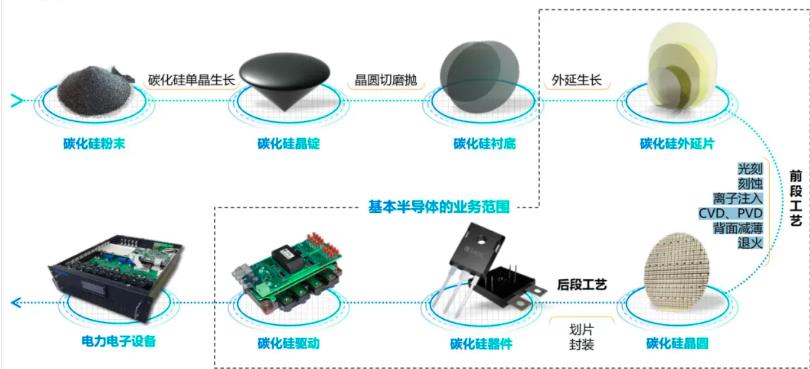
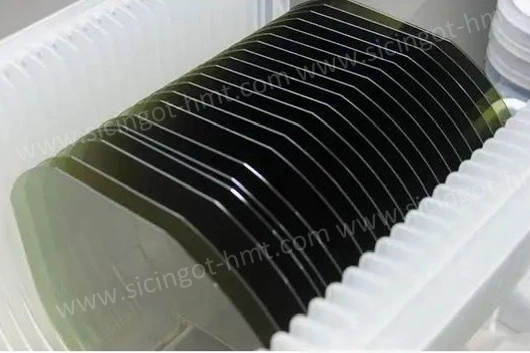
HMT's SiC wafer production covers multiple stages from SiC boule growth to wafer slicing, lapping and polishing. This integrated process allows the substrate geometry and surface condition to be controlled through successive wafer-processing steps.
The standard production route includes crystal growth, wafer slicing, lapping, polishing and final inspection. For a 200 mm wafer, dimensional control becomes particularly important because the wafer diameter is 200 mm and the substrate must maintain suitable geometry throughout subsequent semiconductor processing.
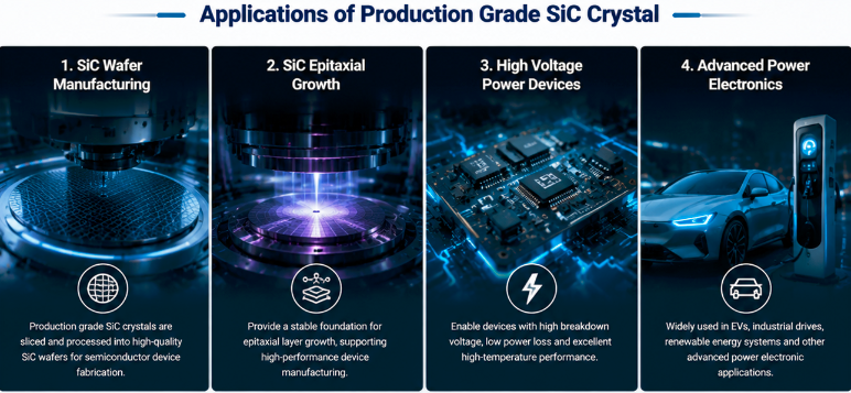
Applications of 8 Inch 4H-N SiC Wafers
Our 8-inch SiC substrates reduce per-chip manufacturing cost by up to 35% compared to 6-inch substrates due to higher die yield per wafer. The thermal conductivity reaches >350 W/m·K, which reduces power device junction temperatures by up to 40°C during high-power switching. Integrated vertical manufacturing from SiC boule growth to Chemical Mechanical Planarization (CMP) guarantees 99.8% batch-to-batch consistency.
The 200 mm 4H-N SiC substrate is suitable for power semiconductor development, SiC MOSFET process development, diode technology, epitaxial wafer preparation and advanced SiC device research. The N-type conductivity and defined resistivity range make the substrate suitable as a starting material for processes where electrical substrate properties are important.
The 8 inch format is particularly relevant to customers evaluating larger-wafer SiC manufacturing because its 200 mm diameter provides substantially more wafer area than 100 mm and 150 mm formats. Final suitability should be determined from the required voltage class, epitaxial structure, defect specification and device process.
Related SiC Substrate Products
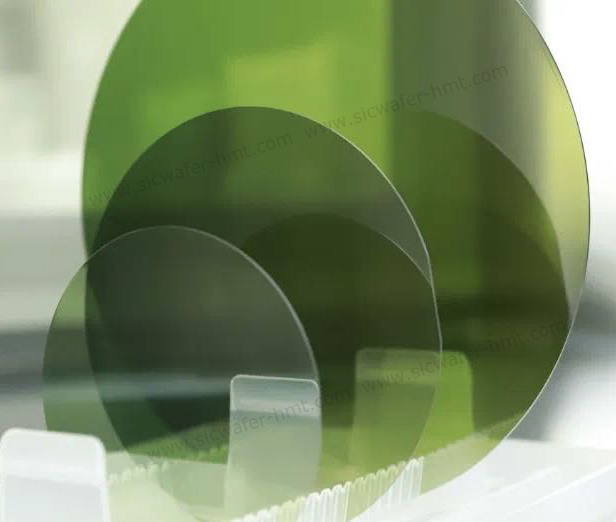
Customers comparing wafer sizes can also review HMT's 6 inch SiC wafer, 4 inch SiC substrate and 2 inch SiC wafer options. Customers evaluating material quality can compare production-grade, dummy-grade, HPSI and epi-ready SiC substrates according to process requirements.
Q1: What is the main application of P Grade 8 inch 4H-N SiC wafers?
A1: P Grade (Production Grade) 8-inch SiC wafers are engineered for commercial power device fabrication, including MOSFETs, Schottky barrier diodes (SBDs), and EV traction inverters requiring high breakdown voltages up to 1200V.
Q2: How does HMT ensure the thickness tolerance of 200mm SiC substrates?
A2: HMT utilizes advanced multi-wire diamond slicing and automated Chemical Mechanical Polishing (CMP) lines, achieving a 500μm ±25μm thickness tolerance with TTV (Total Thickness Variation) under 5μm.
Q3: What is the lead time and Minimum Order Quantity (MOQ) for 8-inch SiC wafers?
A3: Standard sample orders start at 10 piece with a quote turnaround time of <72 hours, while volume production batches (50+ wafers) are dispatched within 6-8 weeks depending on customized resistivity requirements.
Related Products


 E-mail: kim@homray-material.com ; tina@homray-material.com
HMT Gallium Nitride (GaN) Wafer Website: www.ganwafer-hmt.com