
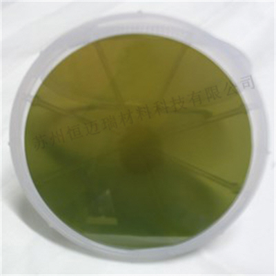
Conductive N 4H-SiC Wafer Manufacturer
Type: 4H-N
Grade: D R P
Thickness: 350um±25um
Dimension: 2 inch~8 inch
Product Description
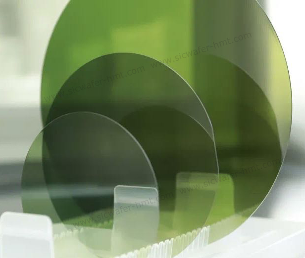
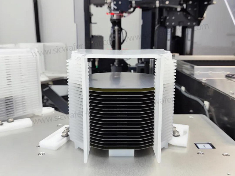
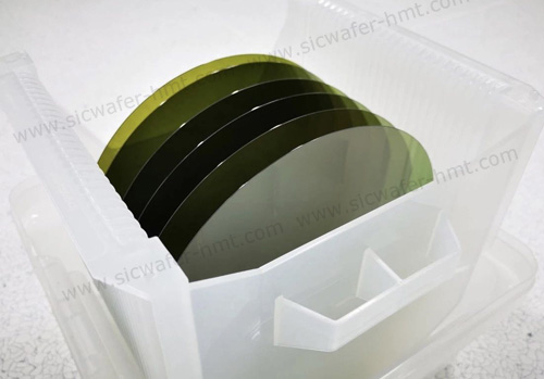
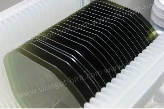
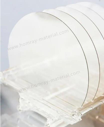
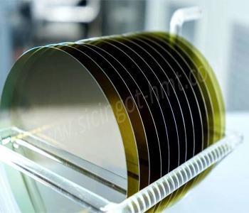
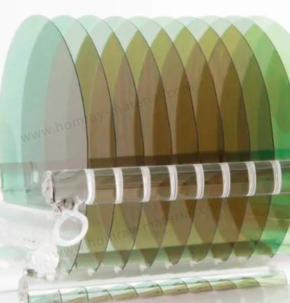
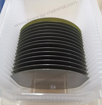
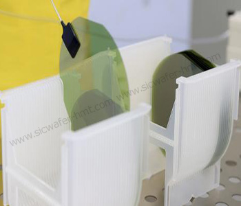
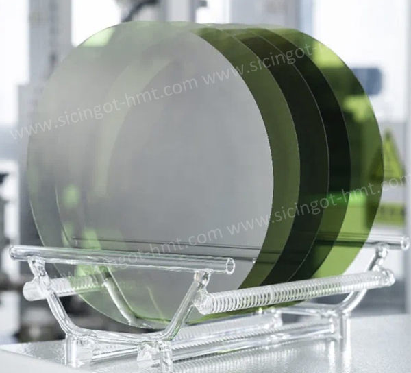
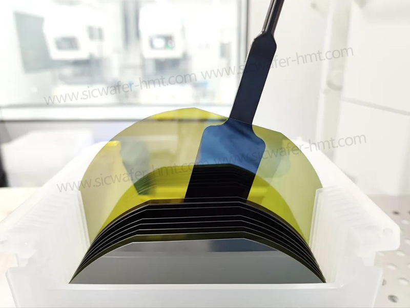
Homray Material Technology (HMT)-a certified manufacturer of semiconductor-grade 4H-silicon carbide substrates - delivers precision-engineered conductive N-Type 4H-SiC wafers across all commercial sizes (2", 4", 6", and pilot 8"). Our substrates feature:
-
Standard thickness: 350μm ±25μm (industry-standard epi-ready)
-
Seed substrate thickness: 500μm ±25μm (optimized for crystal growth)
-
Micropipe density: < 0.5 cm⁻²
-
Resistivity control: 0.015-0.028 Ω·cm
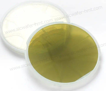
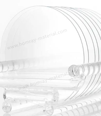
SiC Substrate Basic Spec
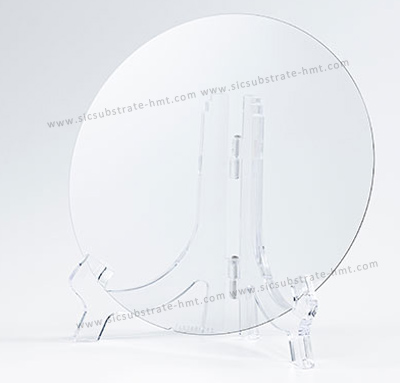
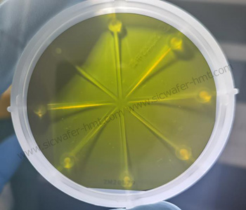
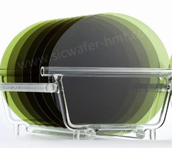
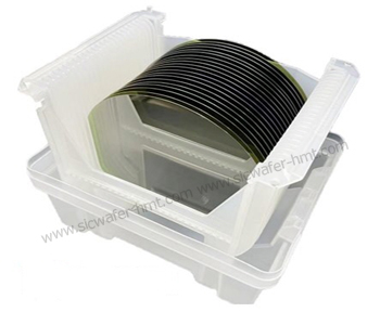
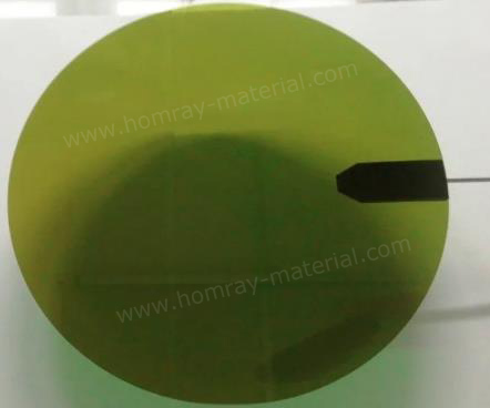
Dimension:2 inch 4 inch 6 inch 8 inch
Thickness: 350um 500um
Dopant: Conductive N nitrogen
Resistivity: 0.015-0.028ohm.cm
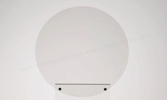
Orientation: off axis 4.0 toward<1120>±0.15°
Grade: D grade R grade P grade
MPD: Different grade has different MPD parameters
Surface: Si face CMP C face polished


At present, SiC material epitaxy is mainly to control the thickness of epitaxy and doping concentration of two parameters. The epitaxial parameters are different according to different device designs. Generally speaking, the larger the thickness of epitaxial, the higher the voltage that the device can withstand, but the larger the thickness of epitaxial layer, the more difficult it is to prepare high quality epitaxial chip, especially in the field of high voltage, it is very difficult to control defects.
SiC wafer after epitaxial growth is mainly used to manufacture power devices, radio frequency devices and other discrete devices, can be widely used in new energy vehicles, 5G communications, photovoltaic power generation, rail transit and other modern industrial fields.
Related Products


![]() E-mail: kim@homray-material.com ; tina@homray-material.com
E-mail: kim@homray-material.com ; tina@homray-material.com
HMT Gallium Nitride (GaN) Wafer Website: www.ganwafer-hmt.com