
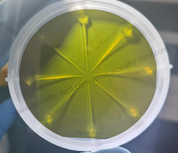
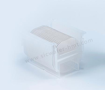
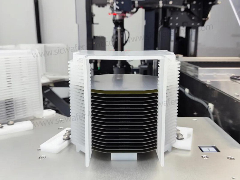
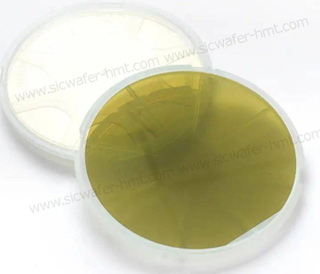
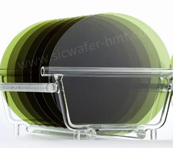
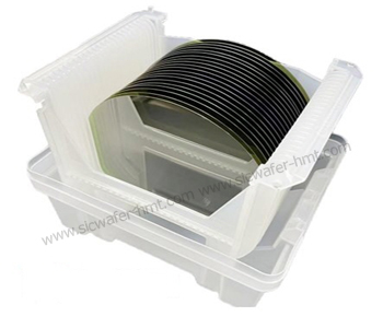
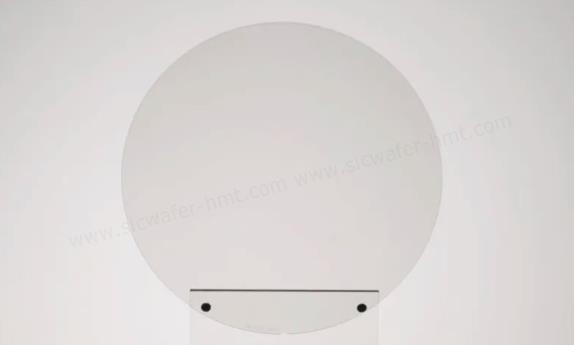
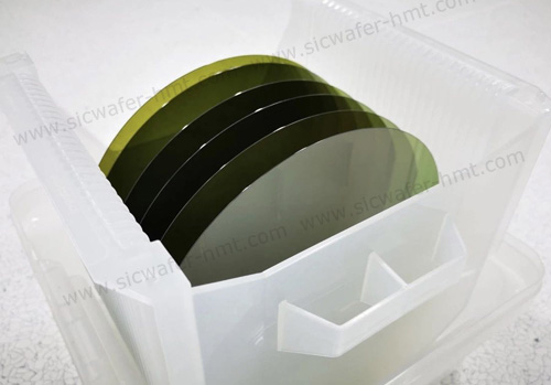
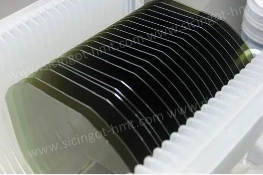
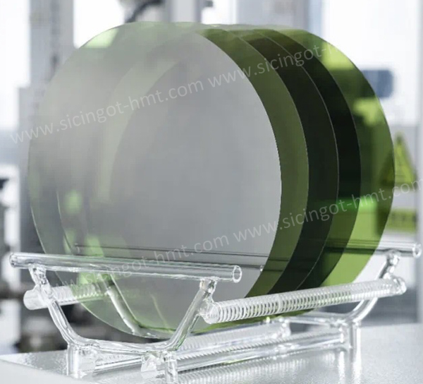
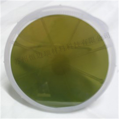
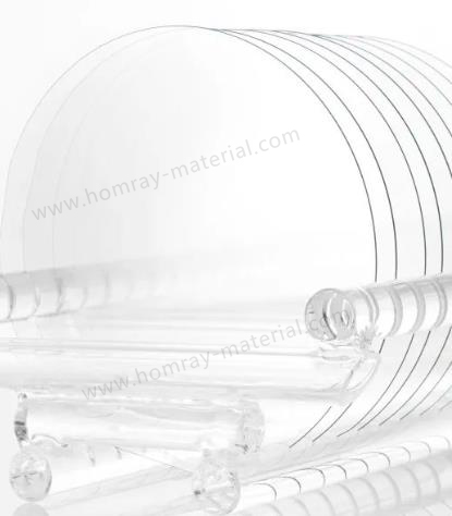
4Inch 4H-SiC Wafers Manufacturer Conductive & Semi-Insulating
Grade: D/R/P Grade
Type: 4H-N/4H-HPSI
Dimension: 4inch
Thickness:350±25um
Product Description
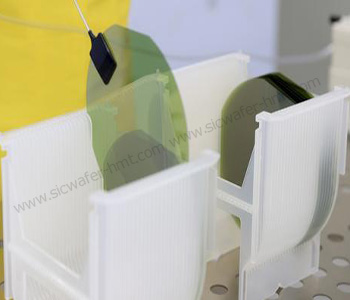
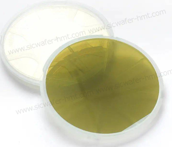
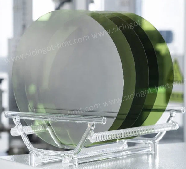
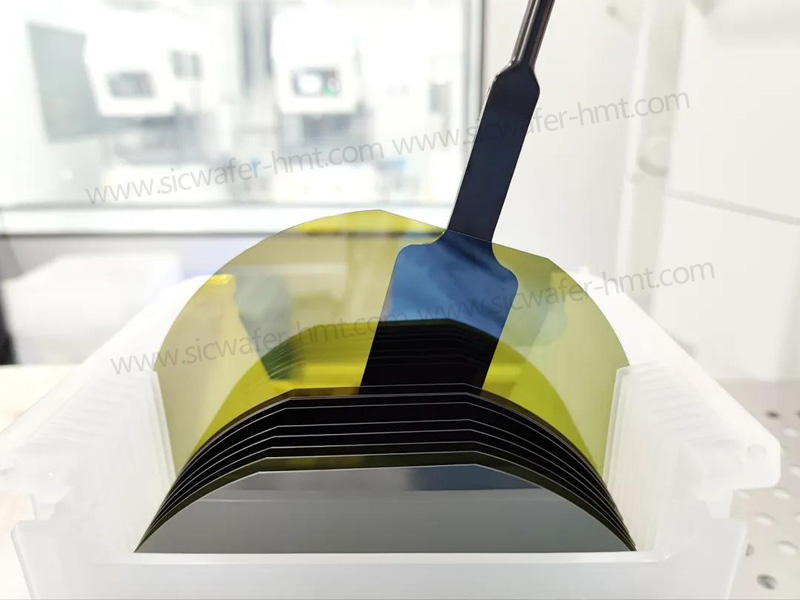
4 Inch 4H-SiC Substrate for Semiconductor Applications
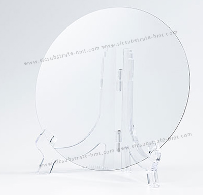
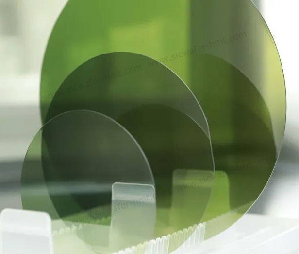
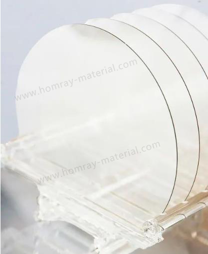
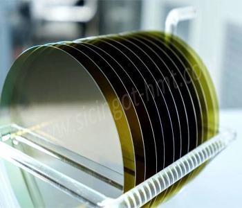
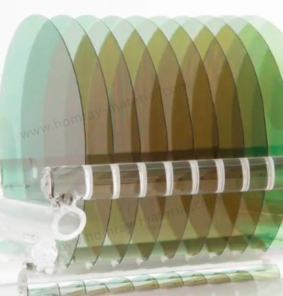
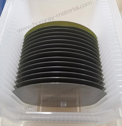
A 4 inch 4H-SiC substrate provides a practical 100 mm platform for semiconductor research, process development and device-related material evaluation. Compared with larger wafer formats, the 4 inch size remains useful for projects that require a mature wafer diameter while maintaining manageable material consumption and process costs.
HMT provides 100 mm 4H-SiC substrates in conductive and semi-insulating configurations. The substrate specification can be selected according to electrical requirements, surface condition, thickness and intended semiconductor process.
100 mm 4H-SiC Substrate Specifications
The standard configuration available from HMT includes a 4 inch wafer diameter with application-specific thickness and electrical characteristics.
| Parameter | Conductive 4H-SiC | Semi-Insulating 4H-SiC |
| Wafer Diameter | 100 mm / 4 inch | 100 mm / 4 inch |
| Crystal Structure | 4H-SiC | 4H-SiC |
| Material Type | N-Type Conductive | Semi-Insulating |
| Typical Thickness | 350 ± 25 μm | 500 ± 25 μm |
| Typical Thickness | 0.015–0.028 Ω·cm | ≥1 × 10⁸ Ω·cm |
| Wafer Grade | D / R / P* |
D/R/P* |
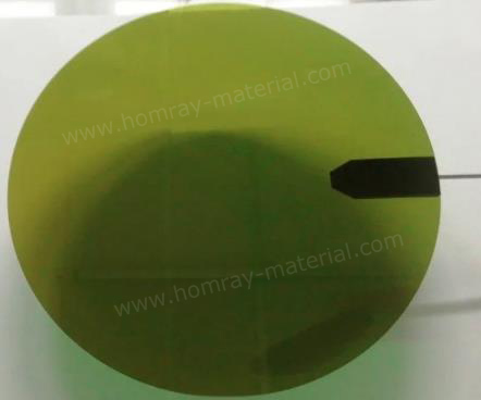
Conductive 4 Inch 4H-SiC Substrate
Conductive 4H-SiC substrates are commonly selected when the substrate needs to provide a defined electrical path for semiconductor device fabrication and related process development.
The conductive configuration can be specified according to parameters such as 4H crystal structure, N-type conductivity, resistivity, thickness, orientation and surface finish.
For customers developing or evaluating SiC-based power devices, the 100 mm format provides a useful intermediate platform between small research wafers and larger-volume wafer formats.
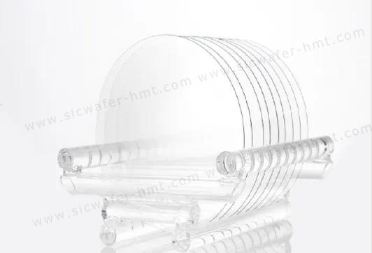
Semi-Insulating 4 Inch 4H-SiC Substrate
Semi-insulating 4H-SiC substrates are designed for applications where high substrate resistivity is important.The semi-insulating configuration offered for this product is based on a typical thickness of 500 μm and resistivity of ≥1 × 10⁷ Ω·cm, subject to the final specification.
These substrates can be considered for RF-oriented semiconductor development, microwave device research and other processes where substrate electrical isolation is an important material consideration. For customers evaluating RF structures on SiC, the 4 inch format offers a practical 100 mm platform for process development and prototype fabrication.
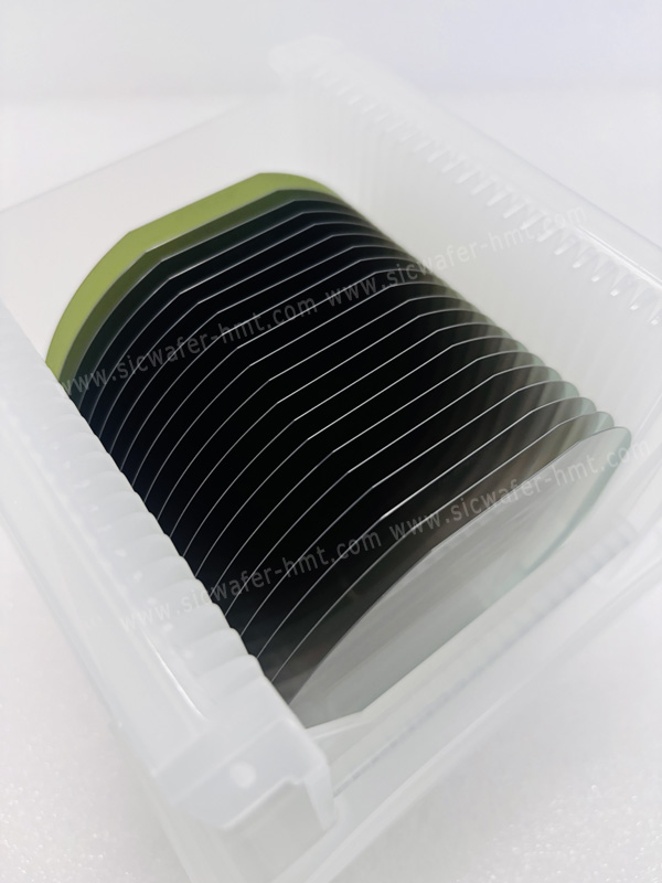
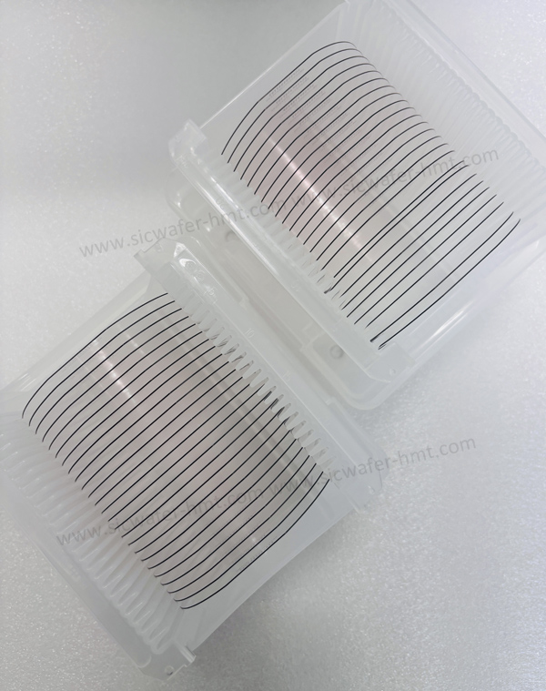
4 Inch SiC Wafer for Research and Process Development
A 4 inch SiC substrate is particularly suitable for semiconductor laboratories, prototype development and process evaluation where a 100 mm wafer format is already supported by existing equipment.
Typical development activities may include:
- SiC power device process development
- MOSFET and Schottky diode research
- RF and microwave material evaluation
- Epitaxial growth studies
- Surface processing experiments
- Wafer fabrication process development
- Semiconductor material characterization
The actual suitability of a substrate should be determined by the electrical, crystalline, geometrical and surface requirements of the specific process.

4H-SiC Substrate Selection: Conductive or Semi-Insulating?
The choice between conductive and semi-insulating material depends primarily on the electrical structure of the intended device or experiment.
Conductive 4H-SiC is generally considered when controlled substrate conductivity is required.
Semi-insulating 4H-SiC is more appropriate when high substrate resistivity and electrical isolation are important to the application.
Selecting the correct substrate configuration at the beginning of a project can help avoid unnecessary process adjustments later.
Why Use a 4 Inch SiC Substrate?
The 4 inch format remains relevant even as the semiconductor industry moves toward larger wafer diameters. For projects using a smaller wafer format, customers can also compare this platform with our 2 inch 4H-SiC wafer option.
A 100 mm SiC substrate can be useful when:
- A mature and established wafer format is required
- Research equipment is configured for 4 inch wafers
- Material consumption needs to be controlled
- Prototype or pilot-scale process development is being performed
- Different substrate materials need to be evaluated
- A project is transitioning from small research wafers toward larger formats
The appropriate wafer diameter ultimately depends on the customer's equipment, process flow and development stage. When a larger wafer area is required, customers may also evaluate our 6 inch 4H-SiC substrate configuration.
Request a 4 Inch 4H-SiC Substrate Specification
If you are evaluating a 100 mm SiC substrate for research, process development or device fabrication, provide your required conductivity type, resistivity, thickness, surface finish and wafer grade.
HMT can review the specification and recommend a suitable 4 inch 4H-SiC substrate configuration based on the intended application.
Related Products


 E-mail: kim@homray-material.com ; tina@homray-material.com
HMT Gallium Nitride (GaN) Wafer Website: www.ganwafer-hmt.com