

P Grade 4H-N SiC Wafer Manufacturers
Type: 4H-N
Dimension: 4 inch
Grade: Production
Product Name: SiC Substrate
Product Description
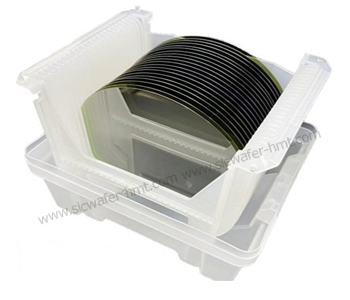
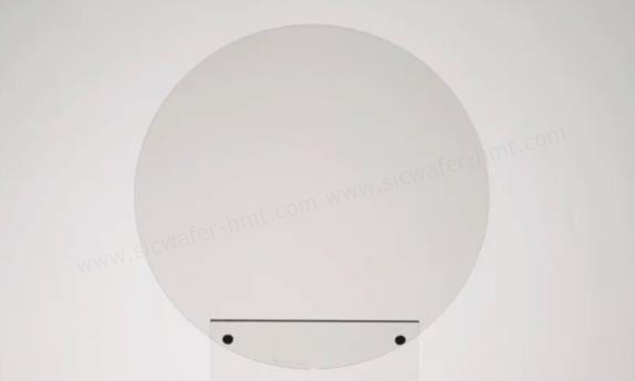
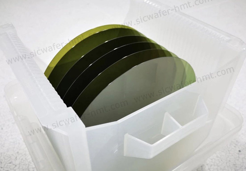
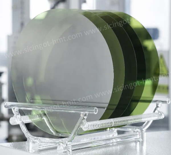
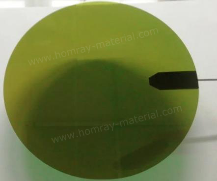
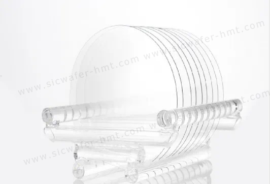
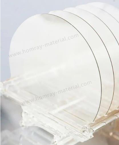
4 Inch P Grade SiC Wafer Manufacturer
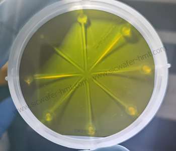
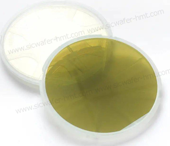
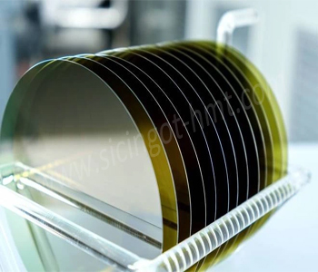
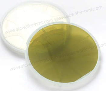
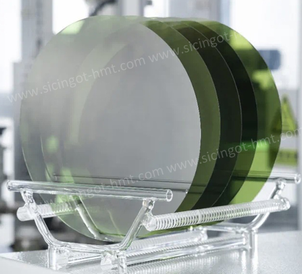
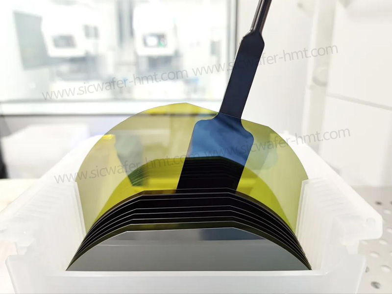
Production-Grade 4H-N Silicon Carbide Substrates
HMT supplies 4-inch P Grade 4H-N silicon carbide (SiC) substrates designed for production-oriented semiconductor applications. This grade is intended for customers who require controlled wafer geometry, thickness uniformity and crystal defect characteristics when preparing SiC substrates for subsequent epitaxial processing and device manufacturing. Key evaluation parameters include total thickness variation (TTV), local thickness variation (LTV), bow, warp and micropipe density (MPD).
Rather than defining P Grade by a single specification, HMT approaches it as a combination of wafer geometry, crystal quality and manufacturing requirements. The final acceptance criteria can be discussed according to the customer's process conditions and technical specifications.
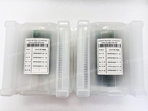
4-Inch P Grade 4H-N SiC Wafer Specifications
The following table summarizes the product's basic configuration. Detailed tolerances and inspection limits should be confirmed against the current manufacturing specification.
| Parameters | Product Information |
| Product | P Grade SiC Substrate Wafer |
| Wafer Diameter | 4 inch |
| Crystal Polytype | 4H |
| Conductivity Type | N-type |
| Product Grade | P Grade-Production Grade |
| Key Geometry Parameters | TTV,LTV,BOW,WARP |
| Crystal Defect Parameter | MPD |
| Surface | Double Side Polished |
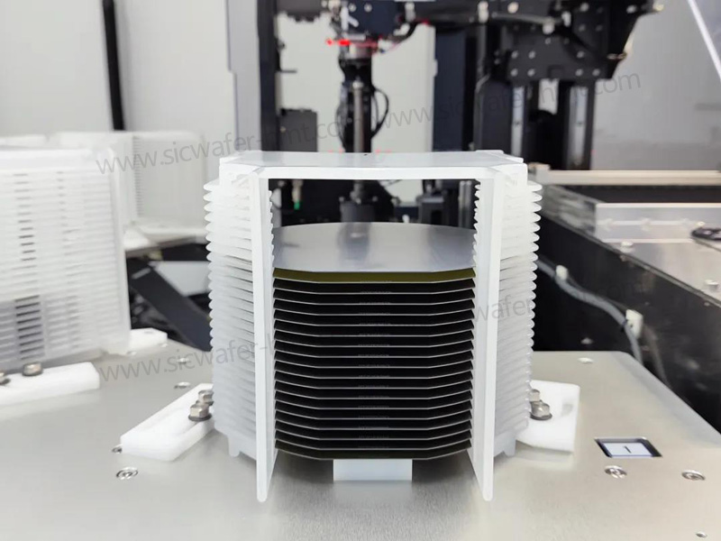
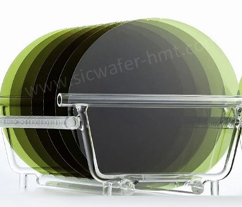
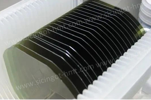
| Package | Cassette |
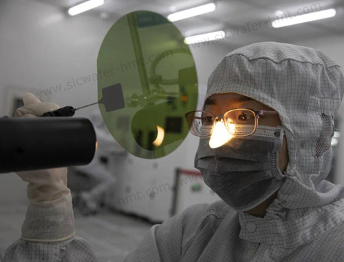
What Defines a Production-Grade P Grade SiC Substrate?
A production-grade SiC wafer needs to meet a coordinated set of physical and material requirements. For customers integrating substrates into repeatable manufacturing processes, wafer geometry and crystal defect characteristics can be as important as the nominal wafer diameter and conductivity type.
For customers comparing different 4-inch SiC substrate grades and configurations, HMT also provides a broader range of 4-inch SiC substrate options.
TTV and LTV: Thickness Uniformity Across the Wafer
Total thickness variation (TTV) describes the difference between the maximum and minimum measured wafer thickness across the specified measurement area. It is an important parameter when evaluating wafer thickness consistency.
Local thickness variation (LTV) provides additional information about thickness changes within defined local regions. Considering TTV and LTV together helps customers assess both overall thickness uniformity and local variations that may affect downstream process control.
Bow and Warp: Wafer Geometry
Bow and warp describe different aspects of wafer shape. Bow represents the wafer's center-point deviation from a specified reference plane, while warp describes the overall deviation of the wafer surface from a reference plane.
These parameters matter when evaluating wafer geometry for handling, alignment, mounting and subsequent semiconductor processing. Their acceptable limits depend on the customer's equipment, process flow and measurement method.
MPD: Micropipe Density
Micropipe density (MPD) is a crystal defect parameter used in the evaluation of silicon carbide substrates. Micropipes are commonly assessed because their presence can affect the suitability of a substrate for certain semiconductor device structures.
For production-oriented substrates, MPD should be considered together with other relevant crystal quality indicators and the customer's device requirements. HMT can discuss the applicable MPD inspection criteria as part of the product specification.

Applications of 4-Inch P Grade 4H-N SiC Substrates
4H-N SiC substrates are used as a starting material for semiconductor structures that take advantage of silicon carbide's wide bandgap properties and high-field performance.
Production-grade substrates can be considered for applications such as:
-
Power semiconductor development: Substrate material for SiC-based power device processes.
-
Epitaxial wafer preparation: Starting substrates for subsequent SiC epitaxial growth, subject to surface and process compatibility.
-
Device process qualification: Material for evaluating wafer handling, process integration and manufacturing consistency.
-
Production-oriented substrate sourcing: Supply programs where wafer geometry and crystal quality requirements need to be specified and inspected.
-
The appropriate substrate configuration depends on the device structure, epitaxial process and downstream manufacturing conditions. Customers are encouraged to provide their intended process requirements when requesting a quotation. For applications requiring a semi-insulating material platform, customers can also explore HMT's [low-MPD HPSI SiC substrates].
Frequently Asked Questions
1. What is a P Grade SiC wafer?
P Grade refers to a production-grade SiC substrate intended for production-oriented applications. Its evaluation considers multiple parameters, including TTV, LTV, bow, warp and MPD, rather than relying on a single quality indicator.
2. What is the difference between P Grade and D Grade SiC wafers?
P Grade and D Grade are different product classifications. Their main differences in HMT's product evaluation relate to wafer geometry parameters such as TTV, bow, warp and LTV, crystal defect characteristics such as MPD, and other inspection considerations. The applicable acceptance limits should be confirmed in the relevant product specification.
Related Products





 E-mail: kim@homray-material.com ; tina@homray-material.com
HMT Gallium Nitride (GaN) Wafer Website: www.ganwafer-hmt.com