
R Grade 6 inch SiC Substrate Wafer Manufacturer
Dimension: 6 inch
Grade: Research Grade
Type: 4H-N ; 4H-SI
Thickness: 350um 500um
Product Description
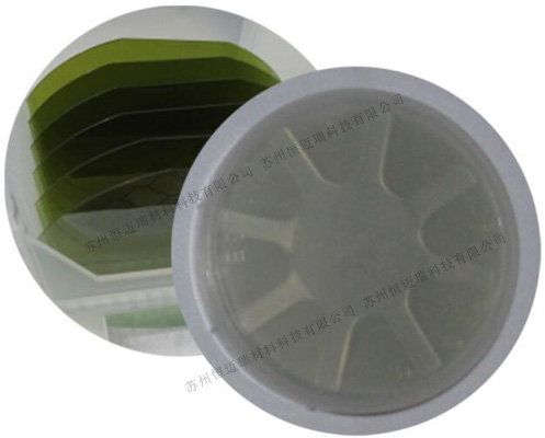
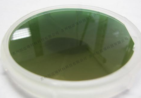
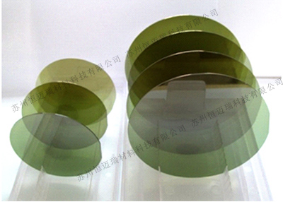
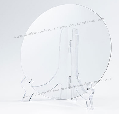
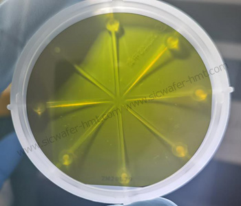
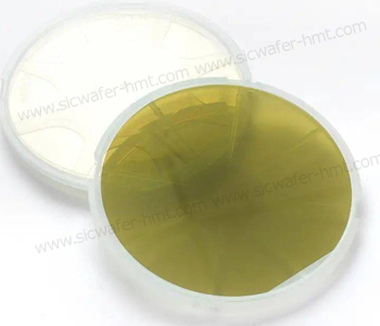
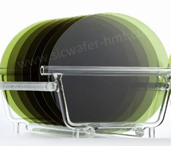
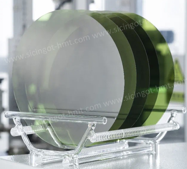
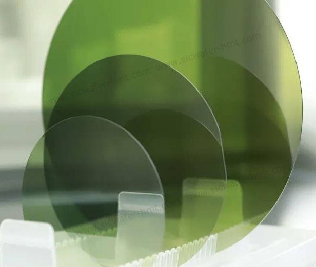
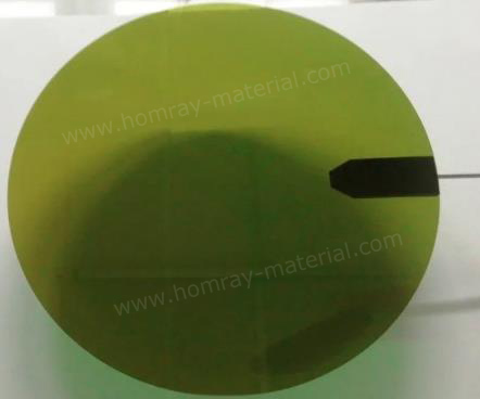
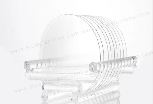
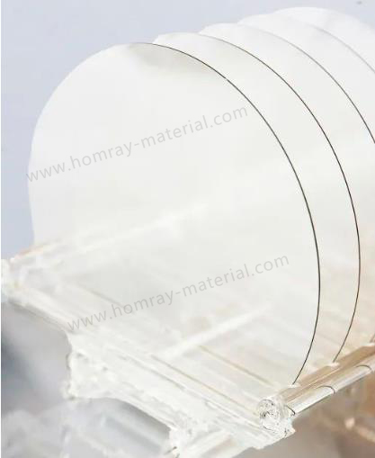
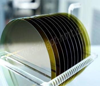
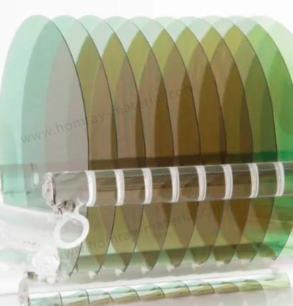
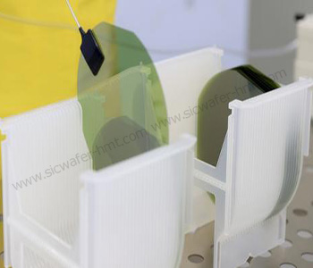
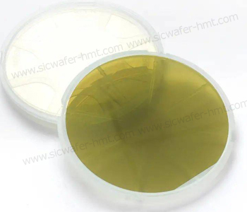
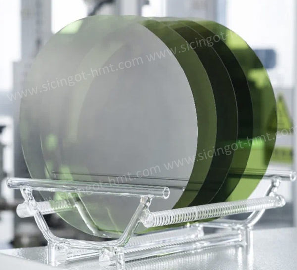
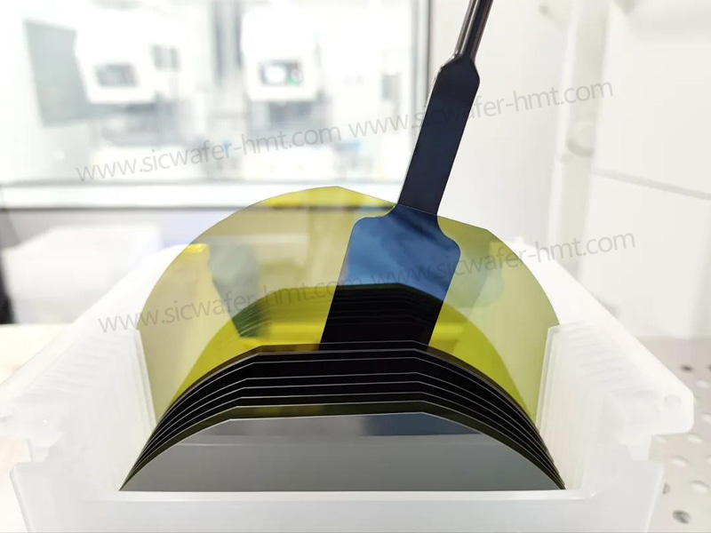
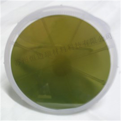
Buy high-quality 6 inch Research Grade SiC Substrate Wafers directly from HMT, a leading Silicon Carbide wafer manufacturer. Specifically designed for university research labs, R&D projects, and semiconductor device testing, our 150mm R Grade SiC substrates offer an exceptionally cost-effective solution for process development. Available in both 4H-N conductive and 4H-HPSI (High-Purity Semi-Insulating) polytypes, these R Grade 6'' SiC wafers provide reliable thermal and structural performance, customizable thickness (350µm–500µm), and low micropipe density (MPD) for non-commercial laboratory trials.
Technical Specifications (150mm / 6 Inch)
| Parameter | 4H N-Type (Conductive) | 4H High-Purity Semi-Insulating (HPSI) |
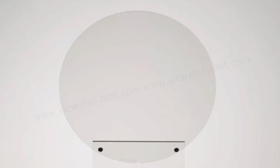
| Diameter | 150.0 ± 0.2 mm | 150.0 ± 0.2 mm |
| Grade | Research Grade (R Grade) | Research Grade (R Grade) |
| Resistivity | 0.015 – 0.028 Ω·cm | >1E7 Ohm.cm |
| Thickness | 350 µm ± 25 µm | 500 µm ± 25 µm |
| Micropipe Density (MPD) | < 1 cm⁻² | < 1 cm⁻² |
| Surface Finish | Double Side Polished (DSP) | Double Side Polished (DSP) |
| Roughness |
≤0.2nm |
≤0.2nm |
| Package |
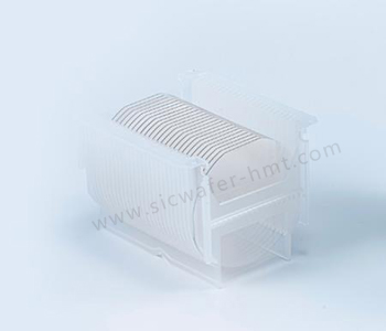
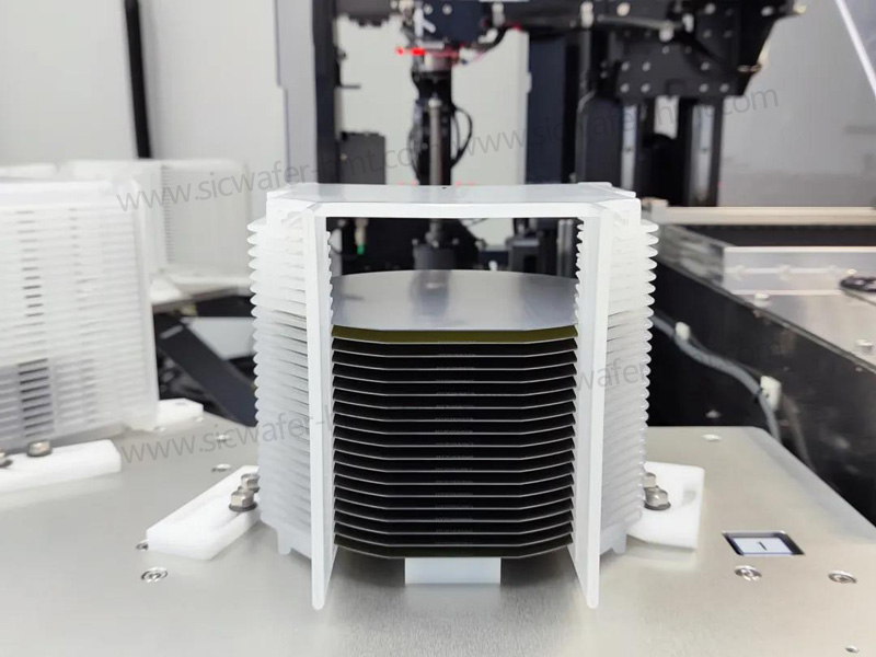
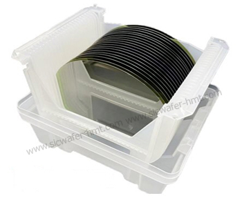
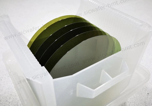
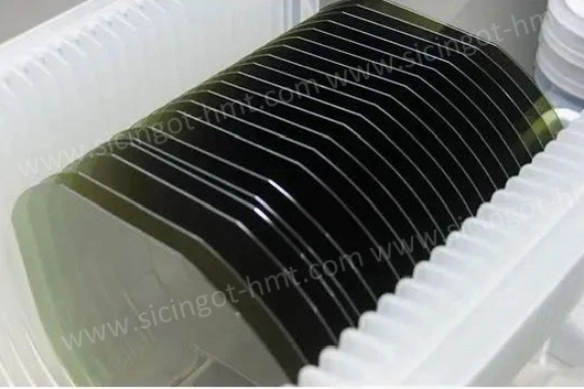
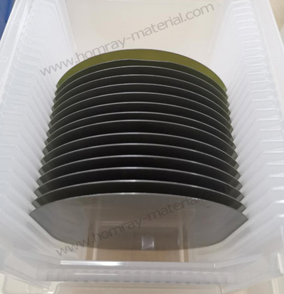
25PCS in one cassette |
25PCS in one cassette |
Why Choose R Grade SiC Wafers for R&D Projects?
While Production Grade (P Grade) SiC wafers are tailored for high-yield commercial power devices and RF fabrication, Research Grade (R Grade) substrates serve an essential role in early-stage semiconductor research:Budget-Friendly Prototyping: Significantly lowers the barrier to entry for experimental trials, photo-lithography testing, and academic thesis projects. Stable Lattice Compatibility: Retains the high thermal conductivity and lattice matching benefits of single-crystal 4H-SiC without the high cost of prime-grade wafers.
If your project requires lower defect counts for mass component production, please explore our high-yield [Production Grade 6 inch SiC Substrate] page.
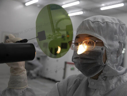
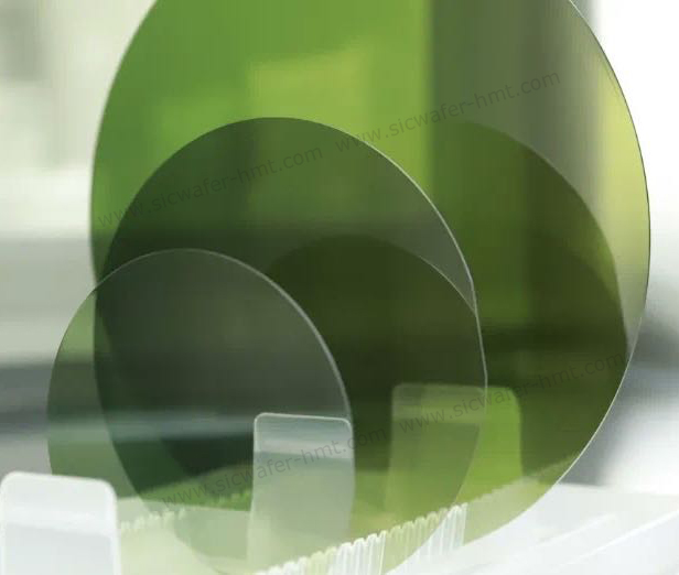
Custom Surface & Edge Processing Options To meet specific experimental requirements, our 6-inch Research Grade SiC substrates can be customized with:
-
Surface Roughness (Ra): < 0.2 nm (CMP polished, Epi-ready finish optional).
-
Orientation Off-cut: On-axis or 4° off-axis toward <11-20> for optimal epitaxial growth.
-
Laser Marking: Custom alphanumeric ID marking on the back or edge for sample tracking during lab processing.
Quality Assurance & Packaging Standards Every batch of 150mm R Grade SiC wafers undergoes strict quality characterization before shipment:
-
X-Ray Diffraction (XRD): Verifies single-crystal lattice orientation and crystal quality.
-
Non-Contact Profilometry: Ensures precise total thickness variation (TTV) and bow/warp control.
-
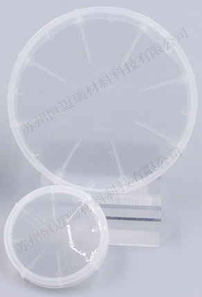
Cleanroom Packaging: Double-bagged under Class 100 cleanroom conditions in anti-static cassette containers to prevent contamination during transit.

Applications & Use Cases
Academic & Institutional Research:Device architecture modeling, material analysis, and optical testing.
Epitaxial Growth Testing:Substrates for GaN-on-SiC and SiC-on-SiC thin-film deposition experiments.
Process Calibration: Ideal for equipment setup, etching rate testing, and ion-implantation tuning.
For advanced heterostructure development, we also supply ready-to-use [SiC Epitaxial Wafers] tailored for power electronics.
Q: What is the main difference between Research Grade (R Grade) and Production Grade SiC Wafers?
A: Research Grade SiC wafers have slightly higher micropipe or defect density compared to Production Grade, making them significantly more economical for non-commercial laboratory testing, process equipment calibration, and preliminary thesis research.
Q: What is the minimum order quantity (MOQ) for Research Grade SiC wafers?
A: We support university labs and startup projects with flexible MOQs.
Related Products

 E-mail: kim@homray-material.com ; tina@homray-material.com
HMT Gallium Nitride (GaN) Wafer Website: www.ganwafer-hmt.com