


4H-SiC Semi-Insulating Substrates
Product Name: Silicon Carbide Substrate
Grade: Ultralow MPD Production Grade
Type: 4H-N ; 4H-SI
Micropipe Density:≤0.1 cm-2
Product Description
HPSI SiC Substrate Manufacturers – 4H-SiC Semi-Insulating Substrates Wafer
HMT is a manufacturer and supplier of 4H-SiC semiconductor substrates, offering 4-inch and 6-inch wafer configurations, including conductive N-type and semi-insulating 4H-SiC materials. For customers seeking HPSI SiC wafer manufacturers, HMT provides substrate options for high-frequency RF devices, GaN-on-SiC epitaxy and advanced semiconductor research, with customized specifications available according to project requirements.
1. HPSI SiC Substrate for High-Frequency Semiconductor Applications
High-Purity Semi-Insulating (HPSI) silicon carbide is an important substrate material for high-frequency semiconductor technologies. Its high electrical resistivity helps reduce unwanted substrate conduction and parasitic electrical effects, making it suitable for RF device structures that require electrical isolation.
Unlike conventional conductive N-type SiC substrates, HPSI 4H-SiC is selected primarily for its electrical insulation characteristics and compatibility with III-nitride epitaxial structures.
HMT supplies semi-insulating 4H-SiC substrate configurations for customers developing GaN-based RF transistors, microwave components and high-frequency semiconductor devices. The final material selection can be based on resistivity, crystal orientation, wafer diameter, thickness and surface requirements.
2. 4H-SiC Substrate Specifications
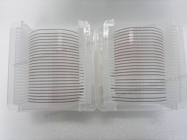
HMT offers 4-inch and 6-inch silicon carbide substrates with different electrical characteristics and material quality requirements.For customers evaluating different electrical configurations, HMT also provides a dedicated 4 inch 4H-SiC substrate
| Parameters | Product Specification |
| Material | Silicon Carbide(SiC) |
| Polytype | 4H |
| Wafer Diameter | 100mm 150mm |
| Conductivity Type | N-Type / Semi-Insulating (4H-SI) |
| Product Grade | Ultralow MPD Production Grade |
| Micropipe Density | ≤0.1 cm⁻² |
| Wafer Thickness | 350um,500um |
| Resistivity | To be confirmed according to material type and grade |
| Surface Finish | DSP |
| Package | 25PCS in one cassette |
3. HPSI and Conductive 4H-SiC: Understanding the Difference
Selecting the correct electrical type is essential when purchasing a silicon carbide substrate. Although both configurations use the 4H-SiC crystal structure, their electrical characteristics and intended applications are different.
High-Purity Semi-Insulating 4H-SiC
HPSI SiC substrates are designed to provide high electrical resistivity with low unwanted electrical conduction through the substrate.
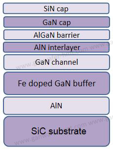
Their material characteristics make them suitable for:
- GaN-on-SiC high-electron-mobility transistors (HEMTs).
- RF power amplifiers and microwave devices.
- High-frequency communication components.
- Radar and aerospace electronic systems.
- III-nitride epitaxial development.
For GaN-on-SiC applications, the semi-insulating substrate provides an electrically isolating foundation for the epitaxial device structure. The combination of GaN's electronic properties and SiC's thermal characteristics makes this material platform attractive for high-power and high-frequency RF applications.
For semiconductor projects requiring a larger wafer format, customers can also explore our 8 inch HPSI SiC substrate.
Conductive N-Type 4H-SiC
N-type SiC substrates are generally selected for applications requiring controlled electrical conductivity.
Typical application areas include:
- SiC MOSFET development.
- Schottky barrier diodes.
- Power semiconductor components.
- SiC-based electronic switches.
- Selected optoelectronic and epitaxial applications.
4. Why Micropipe Density Matters in SiC Wafer Selection
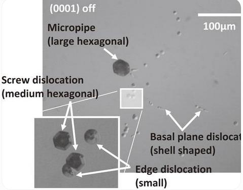 Micropipes are crystallographic defects associated with hollow-core dislocations in silicon carbide single crystals. These defects can propagate into subsequent epitaxial layers and potentially affect semiconductor device fabrication.
For this reason, micropipe density (MPD) is an important parameter when evaluating SiC substrate quality.
HMT provides an ultralow-MPD production-grade 4H-SiC substrate configuration with a specified micropipe density of ≤0.1 cm⁻² for the N-type material.
5. How to Select an HPSI SiC Substrate Manufacturer
When comparing HPSI SiC Substrate manufacturers, buyers should look beyond wafer diameter and price. A reliable material selection process should include several technical considerations.
Electrical resistivity: Confirm the required resistivity range and measurement conditions for the HPSI material.
Crystal quality: Review micropipe density and other relevant dislocation specifications.
Wafer dimensions: Select 4-inch or 6-inch wafers according to the customer's epitaxy equipment and production process.
Surface preparation: Confirm whether single-side polishing, double-side polishing or a specific CMP finish is required.
Wafer geometry: Check thickness, TTV, bow and warp requirements.
Material traceability: Request the applicable inspection data and material documentation for the selected grade.
For customers developing complete semiconductor material structures, HMT also supplies 4H-SiC epitaxial wafers
6. HMT – 4H-SiC Wafer Manufacturer and Supplier
Homray Material Technology (HMT) specializes in silicon carbide crystal materials, SiC substrate wafers and related semiconductor materials.
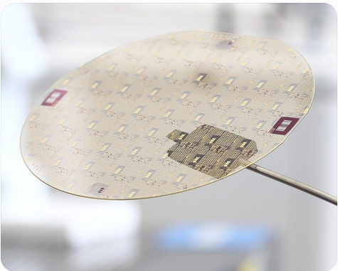
Our product portfolio includes conductive 4H-N SiC substrates, semi-insulating 4H-SiC substrates, ultralow-MPD SiC wafers and SiC epitaxial wafers.
We support 4-inch and 6-inch substrate requirements and can discuss customized material configurations for semiconductor research, epitaxial development and device manufacturing.
Whether you are sourcing HPSI SiC wafers for GaN-on-SiC RF devices or low-MPD SiC substrates for advanced semiconductor processes, HMT can review your technical requirements and provide a suitable product proposal.
Contact HMT for HPSI SiC Substrate specifications, technical documentation and quotation.
Email: kim@homray-material.com
Frequently Asked Questions
Q1. What is an HPSI SiC wafer?
HPSI stands for High-Purity Semi-Insulating silicon carbide. It is a high-resistivity SiC substrate designed to minimize unwanted electrical conduction and support applications such as GaN-on-SiC RF devices and microwave semiconductor components.
Q2. What is the difference between HPSI SiC and conductive N-type SiC?
HPSI SiC is designed for high electrical resistivity and substrate isolation, whereas conductive N-type SiC provides electrical conductivity and is commonly used for power semiconductor devices such as MOSFETs and Schottky diodes.
Q3. What wafer sizes does HMT offer?
HMT provides 4-inch and 6-inch 8-inch SiC substrate configurations for the product range described on this page. Please contact us for availability of a particular electrical type and grade.
Related Products
 E-mail: kim@homray-material.com ; tina@homray-material.com
HMT Gallium Nitride (GaN) Wafer Website: www.ganwafer-hmt.com