


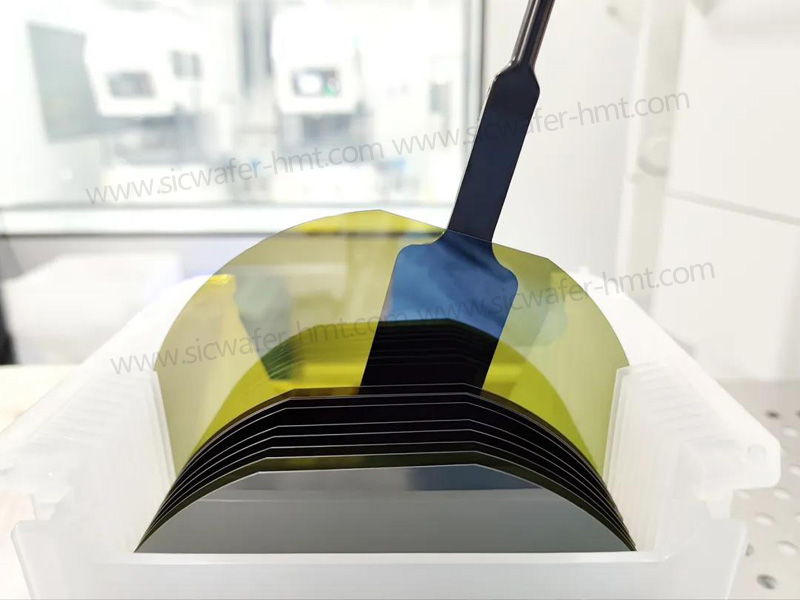
4 inch SiC Substrate Manufacturers
Dimension:4inch
Grade:D/P Grade
Type: 4H-N ; 4H-SI
Thickness: 350um or 500um
Product Description
4 Inch SiC Substrate Manufacturers – 4H-SiC D Grade and P Grade Wafers
HMT is a manufacturer and supplier of 4-inch (100 mm) 4H-SiC substrates, offering D Grade and P Grade silicon carbide wafers in conductive N-type and semi-insulating configurations. With an integrated manufacturing process covering SiC crystal growth, wafer slicing, grinding, lapping, polishing and inspection, HMT provides 4H-SiC substrates for semiconductor research, epitaxial development and power device manufacturing.
1. 4 Inch 4H-SiC Substrate Manufacturing
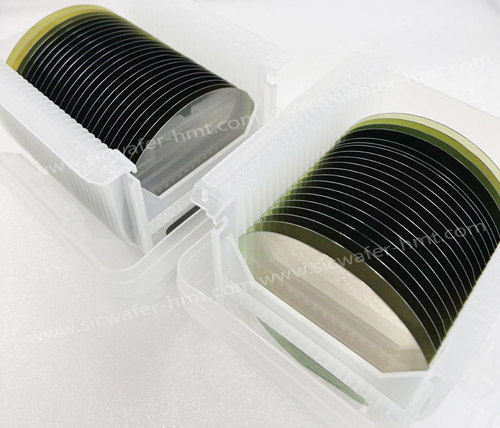
A 4-inch SiC substrate is a 100 mm single-crystal silicon carbide wafer used as a starting material for semiconductor fabrication and epitaxial growth. Its 4H crystal structure and wide-bandgap characteristics make it an established substrate platform for high-voltage, high-temperature and high-frequency electronic devices.
HMT manufactures 4-inch 4H-SiC substrates in different electrical configurations and material grades. Customers can select conductive N-type or semi-insulating 4H-SiC according to their device architecture and processing requirements.
Our 4-inch wafer supply covers D Grade and P Grade material options, supporting customers with different requirements for material quality, surface preparation and production applications.For additional conductive substrate configurations and wafer size options, visit our conductive N-type 4H-SiC wafer.
2. 4 Inch SiC Substrate Specifications
The following table summarizes the available product configurations and the currently specified N-type wafer parameters.
| Parameter | Specification |
| Product | 4 Inch SiC Substrate |
| Wafer Diameter | 100 ± 0.5 mm |
| Crystal Polytype | 4H-SiC |
| Conductivity Type | N-Type / Semi-Insulating |
| N-Type Dopant | Nitrogen |
| Wafer Grade | D Grade / P Grade |
| N-Type Standard Thickness | 350 ± 25 μm |
| N-Type Si-Face | CMP Polished |
| C-Face | Polished |
| Micropipe Density | Depand on different grade |
| Packaging | Cassette |
For a detailed comparison of conductive and semi-insulating material configurations, please refer to our 4 inch 4H-SiC substrate specifications
3. D Grade and P Grade 4H-SiC Substrates
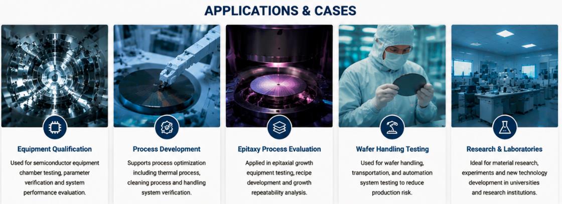
Different semiconductor processes require different substrate quality levels. HMT offers D Grade and P Grade 4H-SiC wafers to support material evaluation, process development and production-related requirements.
D Grade SiC Substrate
D Grade SiC substrates are intended for applications where a defined 4H-SiC material platform is needed for development, testing or process-related evaluation.
Typical uses include:
* Semiconductor process development.
* Wafer handling and equipment evaluation.
* Material characterization.
* Preliminary epitaxial process studies.
* Research and testing applications.
P Grade SiC Substrate
P Grade 4H-SiC substrates are designed for customers requiring production-oriented wafer quality and more clearly defined material acceptance specifications.
They can be considered for:
* SiC epitaxial growth.
* Power semiconductor development.
* MOSFET substrate preparation.
* Schottky diode development.
* Advanced semiconductor process evaluation.
For production applications, buyers should specify the required micropipe density, dislocation density, resistivity, surface roughness, TTV, bow and warp. The final grade acceptance criteria should be confirmed before production.Customers looking for production-oriented material can also explore our 4 inch P Grade SiC wafer.
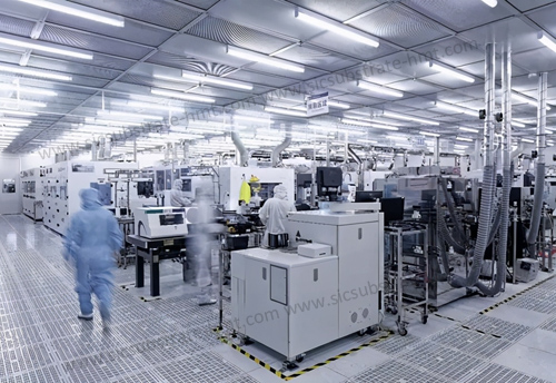
4. From SiC Crystal Growth to Finished 4 Inch Wafer
Consistent substrate quality depends on the manufacturing steps performed between single-crystal growth and final wafer inspection.
HMT's SiC substrate production process covers the following stages:
a. SiC Crystal Growth
High-purity silicon carbide raw materials are used for single-crystal growth. The resulting SiC boule provides the crystalline starting material for subsequent wafer processing.
b. Crystal Processing and Orientation
The SiC crystal is processed to obtain the required diameter and crystal orientation before wafer slicing.
c. Multi-Wire Wafer Slicing
The boule is sliced into individual wafers using precision cutting equipment. Cutting conditions influence the initial wafer geometry and material utilization.
d. Grinding and Lapping
Mechanical processing removes cutting damage and improves wafer thickness uniformity and surface geometry.
e. Polishing and CMP
The wafer surface is processed according to the required finishing condition. The specified N-type configuration uses a CMP-polished Si-face and polished C-face.
f. Inspection and Packaging
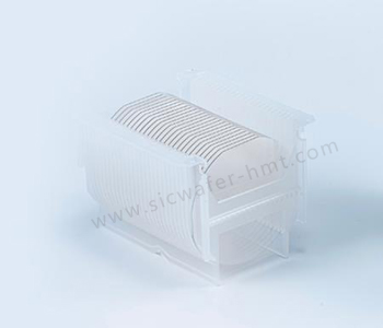
Finished wafers are inspected against the applicable dimensional, surface and material specifications before cassette packaging.
5. Applications of 4 Inch Silicon Carbide Substrates
A 4-inch 4H-SiC wafer provides a practical 100 mm platform for semiconductor research, pilot production and device-related process development.
Its application depends on the electrical type, material grade and epitaxial structure.
SiC Power Electronics
Conductive N-type 4H-SiC substrates are widely used as starting materials for SiC power device epitaxy. Typical device technologies include MOSFETs and Schottky barrier diodes for power conversion and switching applications.
GaN-on-SiC RF Devices
Semi-insulating 4H-SiC provides a substrate platform for GaN-based RF and microwave device structures. Its electrical isolation and thermal characteristics are relevant to high-frequency HEMT development.
Epitaxial Process Development
4-inch SiC wafers are useful for evaluating epitaxial growth conditions, surface preparation and defect behavior before transitioning to larger wafer formats.For customers requiring a processed semiconductor material structure, HMT also provides customized 4H-SiC epitaxial wafers.
Semiconductor Research
Universities, laboratories and semiconductor development teams can use 100 mm SiC substrates for material characterization, process optimization and device fabrication studies.
6. Why Choose HMT as Your 4 Inch SiC Substrate Supplier?
Selecting a 4 inch SiC substrate manufacturer involves more than comparing the nominal wafer diameter. Buyers should evaluate production capability, material consistency, processing conditions and technical communication.
HMT offers several product and manufacturing capabilities:
-
4H-SiC single-crystal substrate supply.
-
100 mm / 4-inch wafer configurations.
-
D Grade and P Grade product options.
-
Conductive N-type and semi-insulating material configurations.
-
Si-face CMP and C-face polishing options.
-
Customized thickness and surface specifications.
-
Cassette packaging and international shipment support.
HMT also supplies 2-inch, 6-inch and 8-inch SiC substrates for customers evaluating different wafer formats. Whether you are sourcing 4-inch SiC wafers for research, epitaxial growth or power semiconductor development, our team can review your technical requirements and recommend an appropriate substrate configuration.
Contact HMT for 4 Inch SiC Substrate Specifications and Quotation
Email: kim@homray-material.com
Email: tina@homray-material.com
Related Products
 E-mail: kim@homray-material.com ; tina@homray-material.com
HMT Gallium Nitride (GaN) Wafer Website: www.ganwafer-hmt.com