
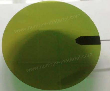
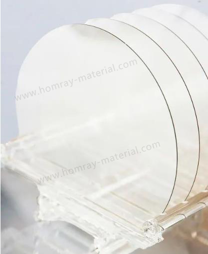
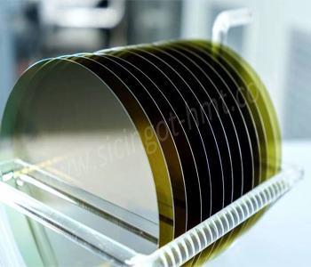
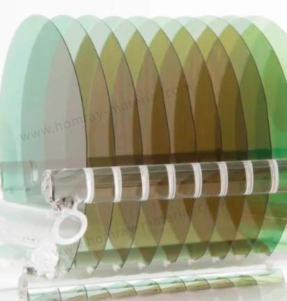
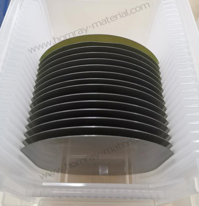
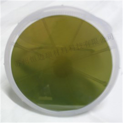
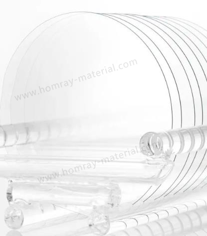
4H-N 8 inch SiC Substrate Manufacturer
Type: 4H-N
Diameter:200mm
Grade: Mechanical
Product Name: SiC Substrate
Product Description
1. Product Overview & Core Specifications
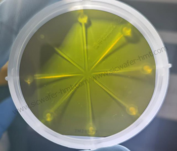
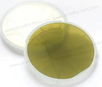
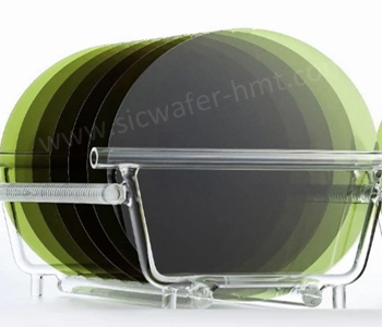
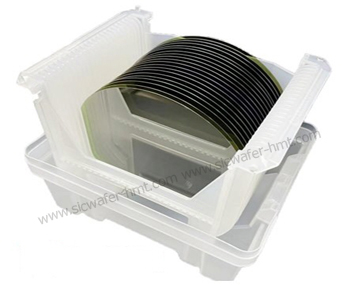
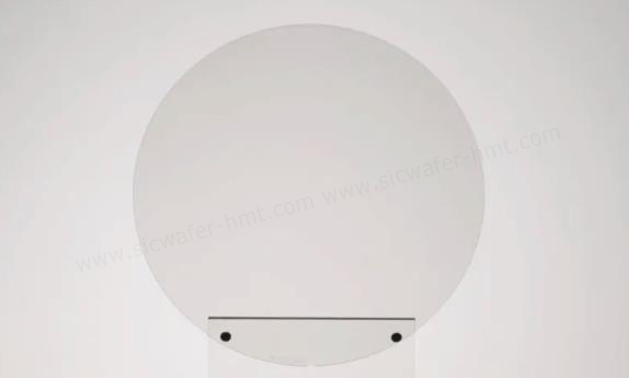
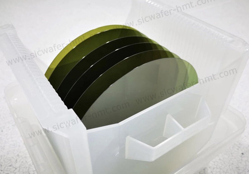
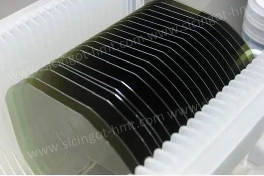
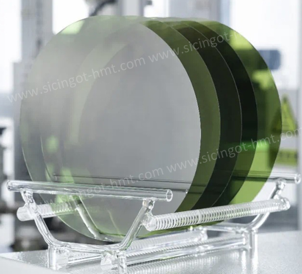
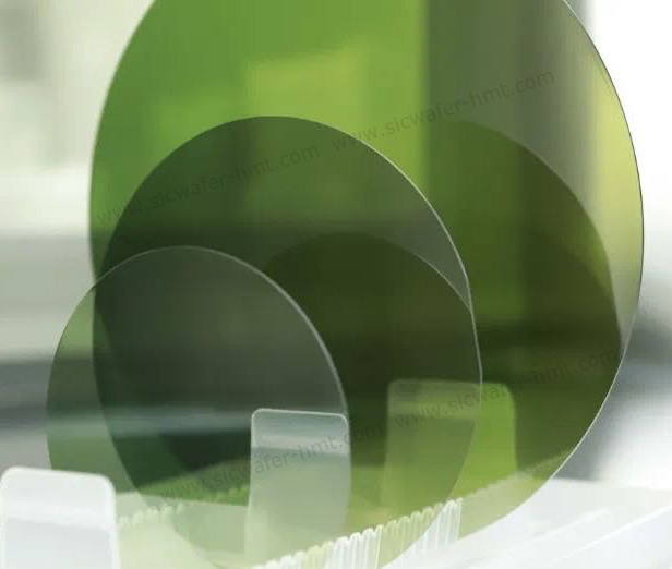
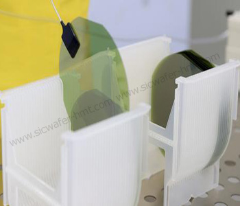
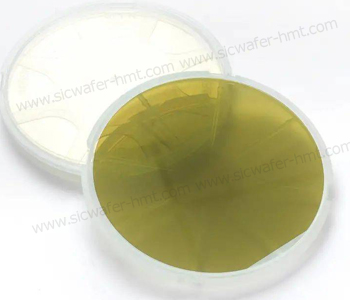
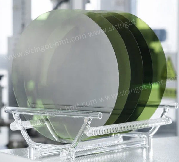
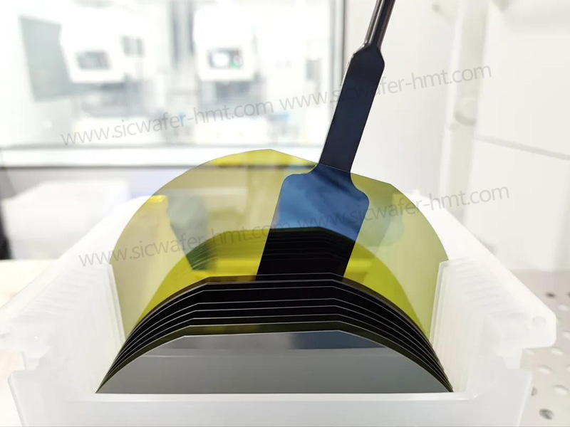
HMT’s 8-inch (200mm) 4H-N conductive silicon carbide (SiC) substrate provides a high-yield foundation for next-generation 1200V–3300V power electronics, including Automotive Traction Inverters and High-Voltage MOSFETs. Fabricated using high-purity Physical Vapor Transport (PVT) crystal growth, each substrate guarantees consistent crystalline lattice orientation with an off-axis angle of 4.0° ± 0.5° toward <1120>. By increasing the usable surface area by nearly 78% compared to standard 6-inch (150mm) wafers, our 8-inch substrates effectively reduce total chip fabrication costs by up to 35%.
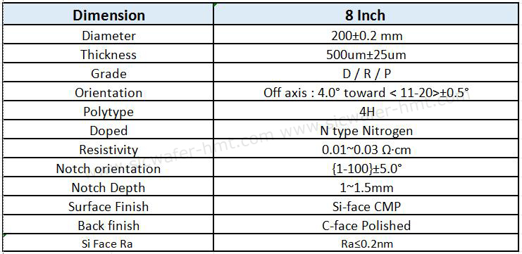
2. Advanced Vertical Manufacturing & Quality Assurance
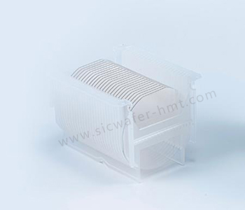
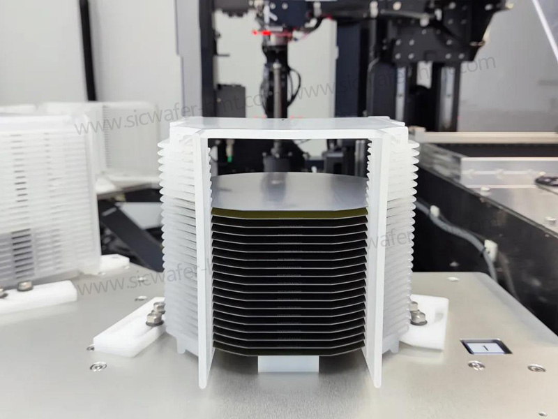
HMT maintains strict vertical control over every stage of the manufacturing process, from raw high-purity SiC powder synthesis to 8-inch SiC boule growth, precision multi-wire diamond slicing, and multi-stage Chemical Mechanical Planarization (CMP). Our automated chemical cleaning and ultra-clean packaging lines ensure that every single wafer meets stringent Class 10 cleanroom standards prior to dispatch.
Our proprietary CMP polishing technology eliminates surface subsurface damage, achieving a scratch-dig specification exceeding 10-5 under high-intensity UV inspection. Every production batch undergoes 100% full-wafer map scanning for electrical resistivity, thickness uniformity, and crystallographic defects, maintaining a 99.8% batch-to-batch consistency rate across all industrial shipments.
3. Thermal Performance & High-Power Density Advantages
With a wide bandgap of 3.26 eV, HMT 4H-N SiC substrates feature a critical breakdown electric field of 2.8 MV/cm, nearly 10 times higher than conventional silicon. This allows device designers to build thinner drift layers with higher doping concentrations, drastically reducing on-state resistance (RDS(on)) and conduction losses in high-voltage MOSFETs and Schottky barrier diodes.
Furthermore, our substrates exhibit exceptional thermal conductivity reaching 490 W/m·K at 300K, allowing power devices to operate reliably at junction temperatures exceeding 175°C without risking thermal runaway. Combined with an electron saturation drift velocity of 2.0×107 cm/s, HMT substrates support high switching speeds above 100 kHz, enabling engineers to downsize passive components and reduce overall inverter cooling systems by up to 40%.
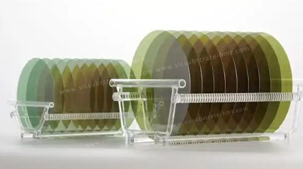
4. Primary Applications & Downstream Integration
HMT's 8-inch 4H-N conductive SiC substrates serve as the ideal platform for growing high-quality homoepitaxial layers used in demanding commercial power switching applications:
-
Automotive Electric Vehicles (EV): Main traction inverters, 800V high-voltage onboard chargers (OBC), and DC-DC converters.
-
Renewable Energy Infrastructure: Commercial solar central inverters, energy storage system (ESS) power conversion, and wind power generation modules.
- Industrial & Smart Grid: High-efficiency industrial motor drives, uninterruptible power supplies (UPS) for data centers, and solid-state transformers for ultra-high voltage power distribution.

Q1: What are the main applications for HMT’s 4H-N 8-inch SiC substrate?
A1: HMT’s 4H-N 8-inch (200mm) conductive SiC substrates are designed for fabricating high-efficiency power devices, including EV traction inverters, 1200V/1700V MOSFETs, Schottky Barrier Diodes (SBDs), and high-voltage ultra-fast smart grid converters.
Q2: How does HMT ensure low micropipe density (MPD) on 200mm SiC substrates?
A2: HMT utilizes optimized thermal field modeling and proprietary PVT crystal growth seed control, maintaining a certified micropipe density (MPD) of less than 0.5 cm⁻² across the full 8-inch surface area.
Q3: What is the standard lead time and sample policy for 8-inch SiC wafers?
A3: Standard sample orders start at a minimum order quantity (MOQ) of 1 piece with guaranteed quotation response within <72 hours, while volume commercial orders (50+ pieces) deliver within 2 to 4 weeks depending on customized resistivity specifications.
Related Products


 E-mail: kim@homray-material.com ; tina@homray-material.com
HMT Gallium Nitride (GaN) Wafer Website: www.ganwafer-hmt.com