

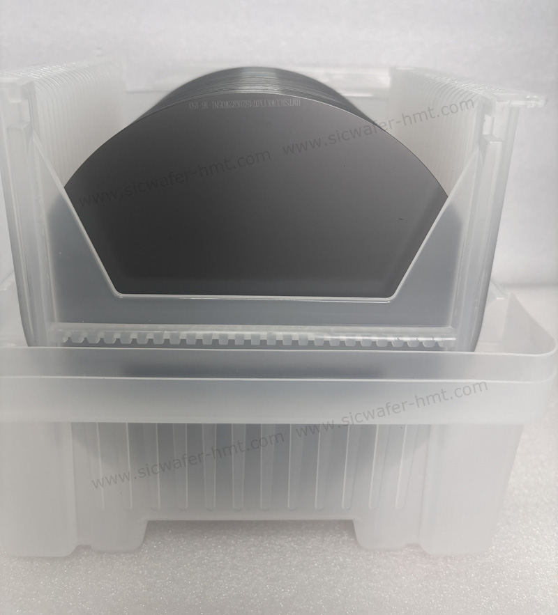
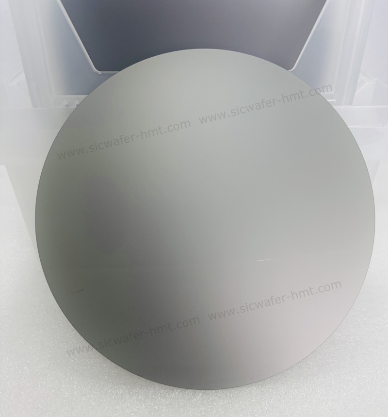
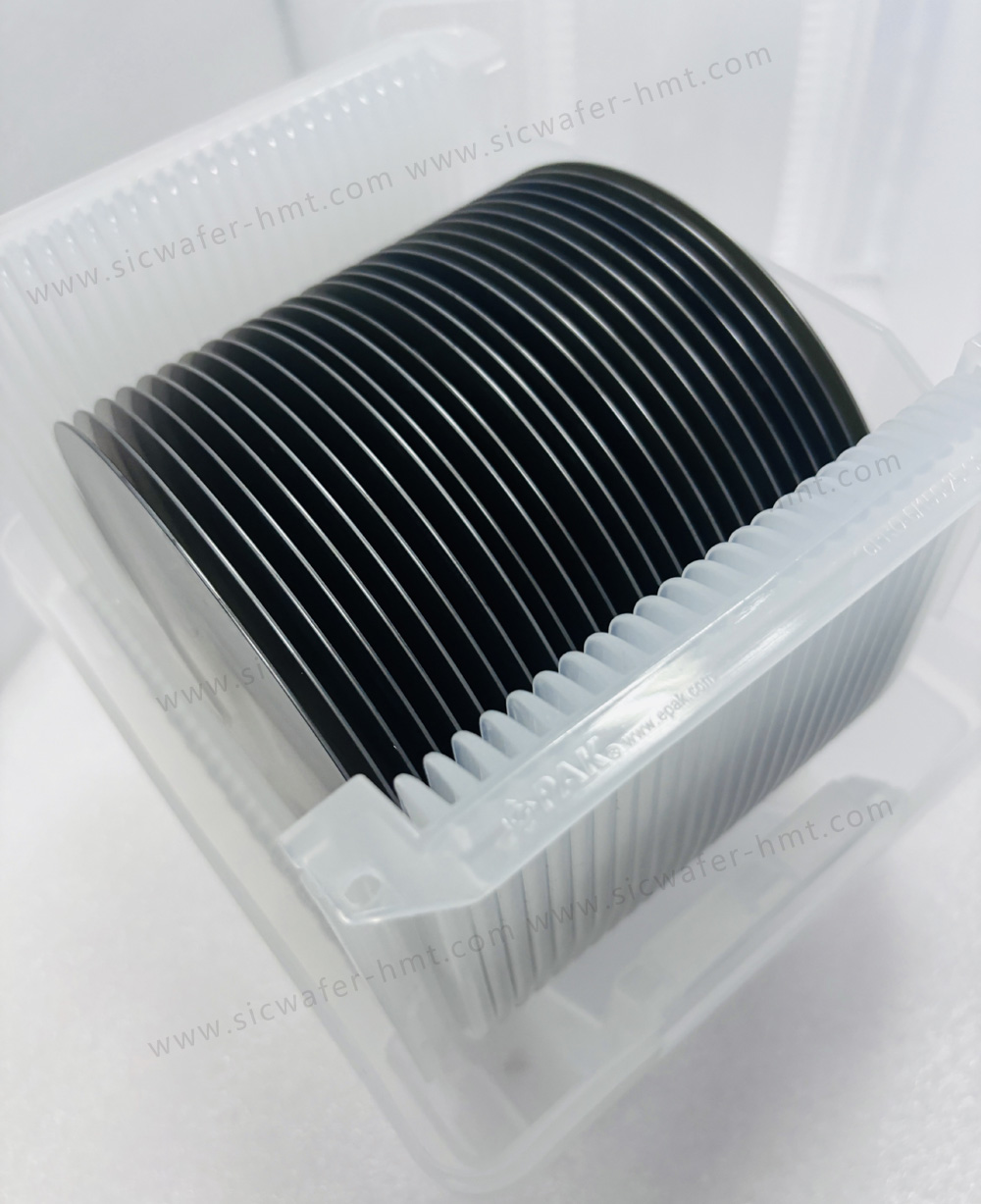
6 inch Unpolished SiC Wafer T-900um
Diameter: 150mm
Type:Conductive N type
Thickness: 900um
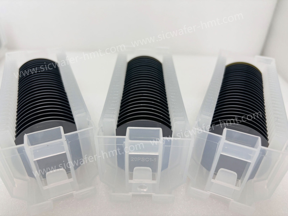
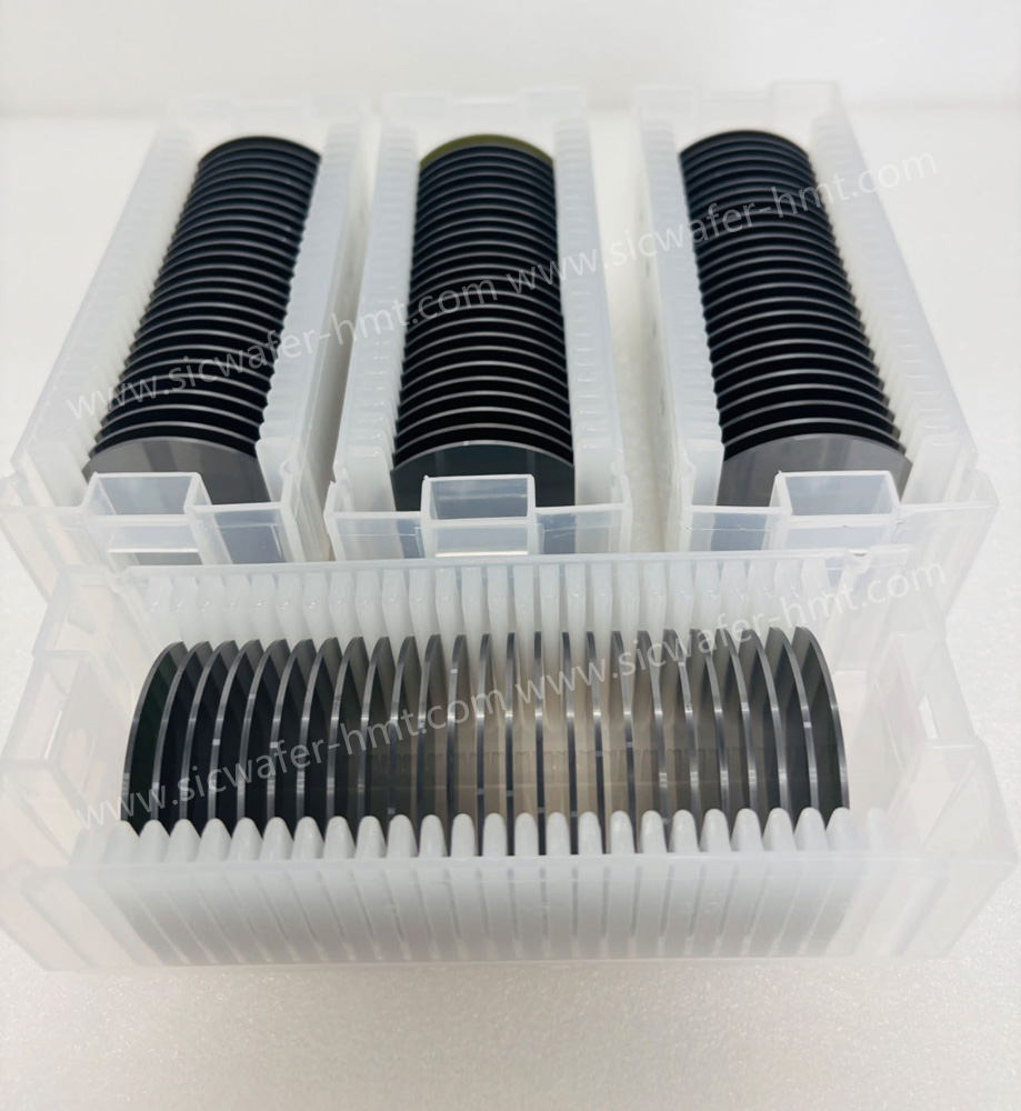
Package: Cassette
Product Description
Are you looking for more thicker SiC unpolished wafer on ther market? Actually, HMT can supply 900um As cut SiC wafer and more thicker SiC slicing wafer upon customer requirement. Normally we have Conductive N type As cut SiC wafer with thickness 400um 500um 600um 900um. We provide high quality Raw cut SiC wafer but very competitive price. If you have diamond grinding wheel testing, grinding or polishing equipment testing, please feel free to contact us now!
6 inch As cut SiC Wafer 6 inch Double side polished SiC Wafer


SiC substrate is the cornerstone of GaN and SiC application in the third generation semiconductor materials. Due to the limitation of technology and process level, large-scale application of GaN material as substrate is still facing challenges. Its application mainly uses sapphire, silicon wafer or semi-insulating SiC wafer as substrate, and fabricate GaN devices by epitaxy growth, which is mainly used in the field of macro station communication radio frequency. The SiC material is mainly in the conductive N type SiC substrate epitaxial growth SiC epitaxial layer, should be used in all kinds of power devices, in recent years, with the maturity of technology and preparation cost, the application in the field of new energy continues to penetrate. SiC material will be the important foundation of SiC and gallium nitride devices in the fields of new energy and 5G communication.
Related Products


![]() E-mail: kim@homray-material.com ; tina@homray-material.com
E-mail: kim@homray-material.com ; tina@homray-material.com
HMT Gallium Nitride (GaN) Wafer Website: www.ganwafer-hmt.com