

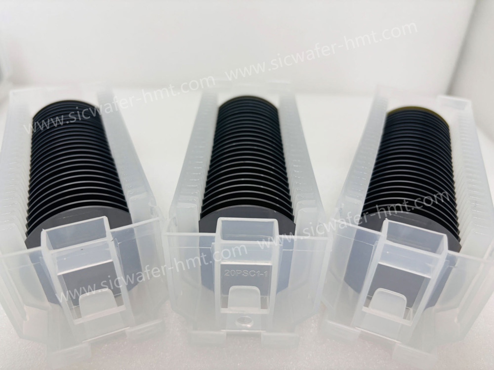
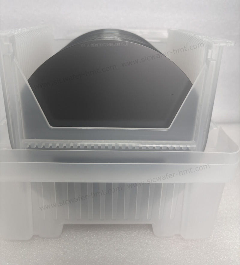
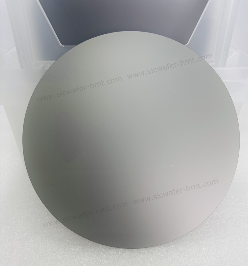
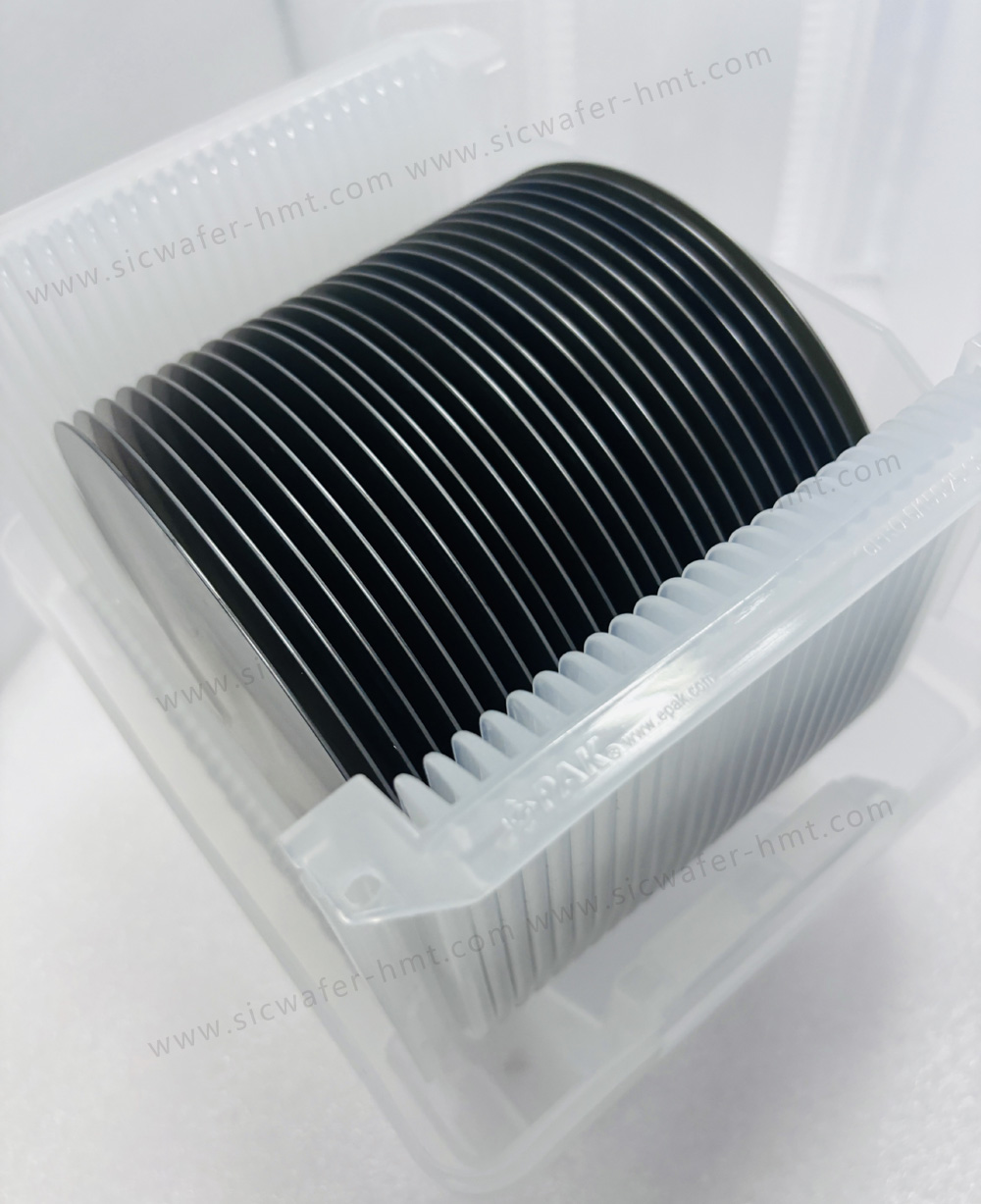
4 inch As-cut SiC Wafer
Diameter: 100mm
Type: SI type Semi-insulated
Thickness: 600um
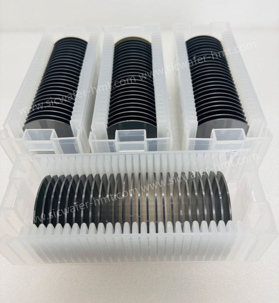
Package: Cassette
Product Description
Homray Material Technology as the un-polished SiC substrate manufacturer and supplier not only provide high quality SiC Ingot and SiC Wafer, but also supply 2inch to 8inch As-cut SiC Substrate. The mainstream is 6 inch and 8 inch raw-cut SiC Wafer, we also can supply 4 inch SiC wafer without polishing. For conductive N type SiC Slicing wafer thickness support customization, and for semi-insulating un-polished SiC wafer is about 600um. Cutomers always purchase raw-cut SiC wafer for testing lapping and polishing machine.


SiC material has wide band gap, high breakdown electric field, high thermal conductivity, high electron mobility and radiation resistance, SiC based SBD and MOSFETs are more suitable for high frequency, high temperature, high pressure, high power and radiation resistance environment. With the same power level, the SiC device can meet the requirements of higher power density and more compact design.
Silicon carbide has a higher power density than traditional silicon wafers, making the size and volume of devices smaller and the corresponding battery size smaller, thus extending battery life and giving electric cars longer range. Tesla's Model 3, for example, uses silicon carbide instead of silicon for its current conversion module.
Related Products


![]() E-mail: kim@homray-material.com ; tina@homray-material.com
E-mail: kim@homray-material.com ; tina@homray-material.com
HMT Gallium Nitride (GaN) Wafer Website: www.ganwafer-hmt.com