


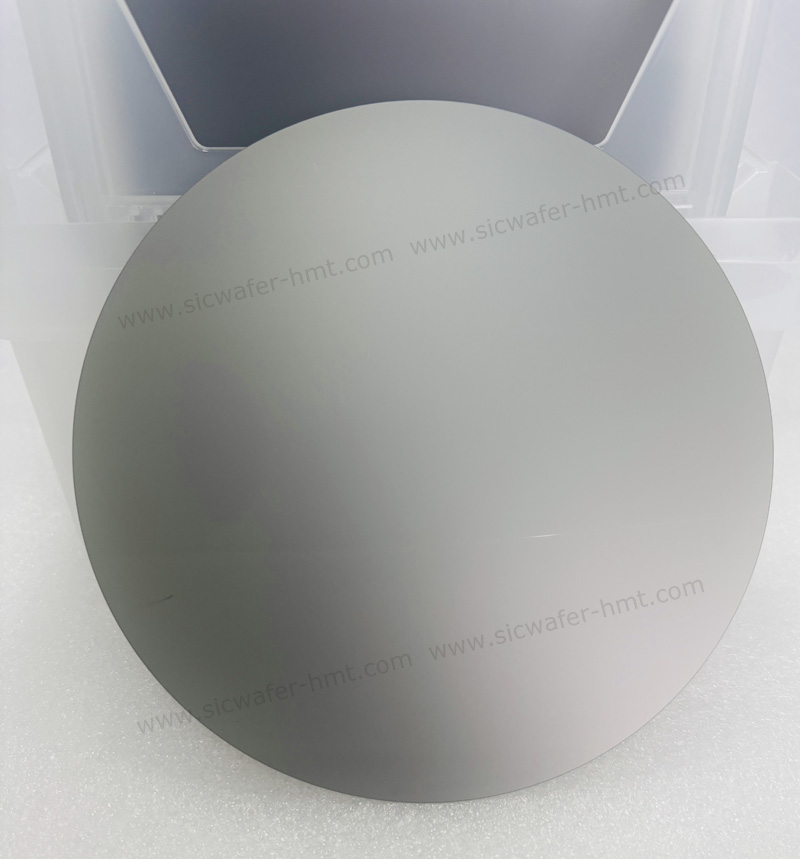
2 inch As Cut SiC Wafer Manufacturer
Type:Conductive N type
Diameter: 2inch / 4inch
Thickness: 600um Customized
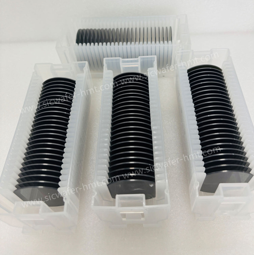
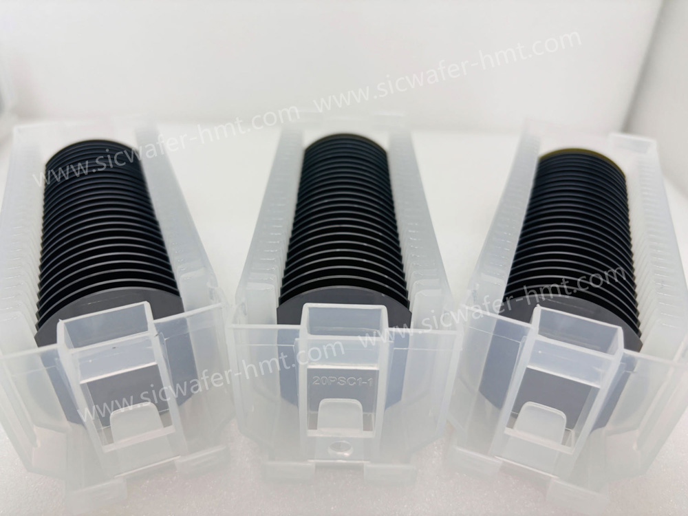
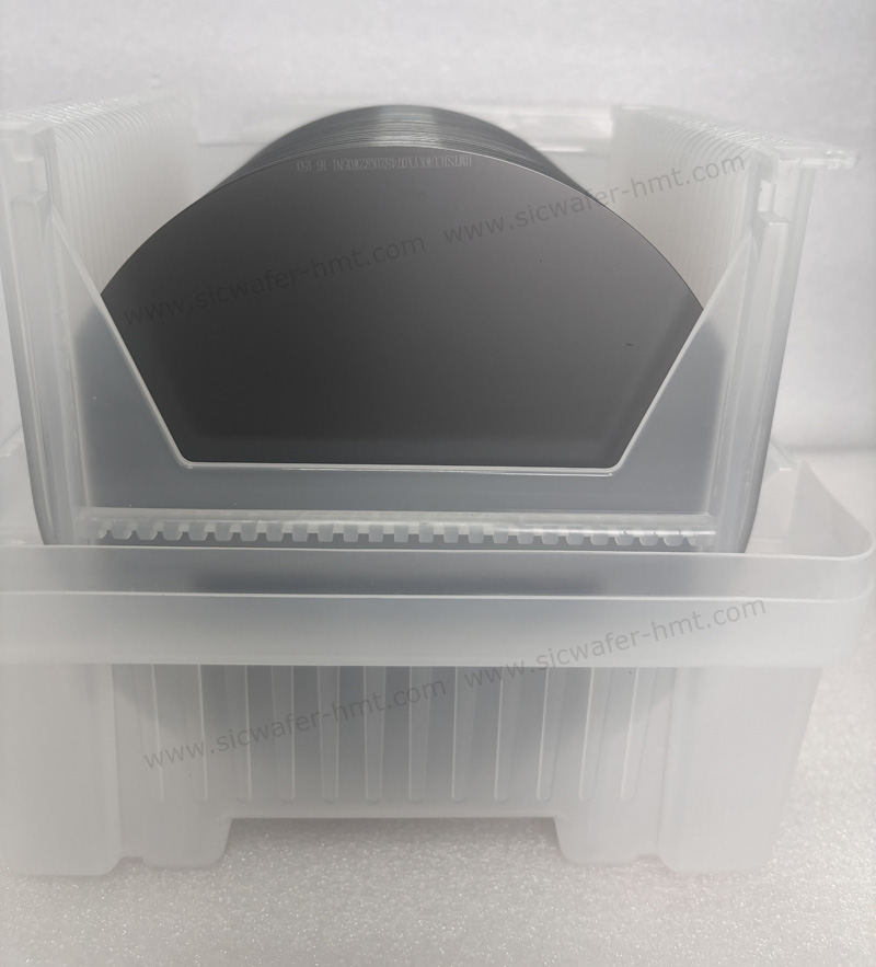
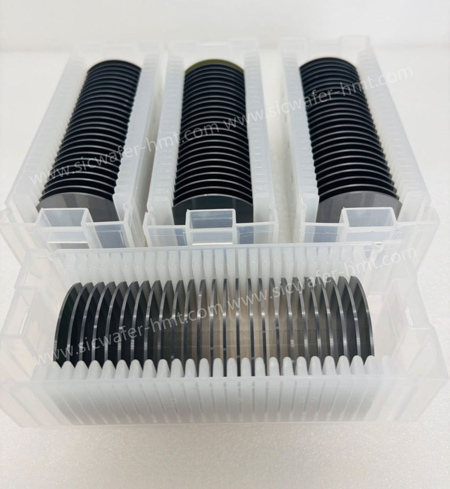
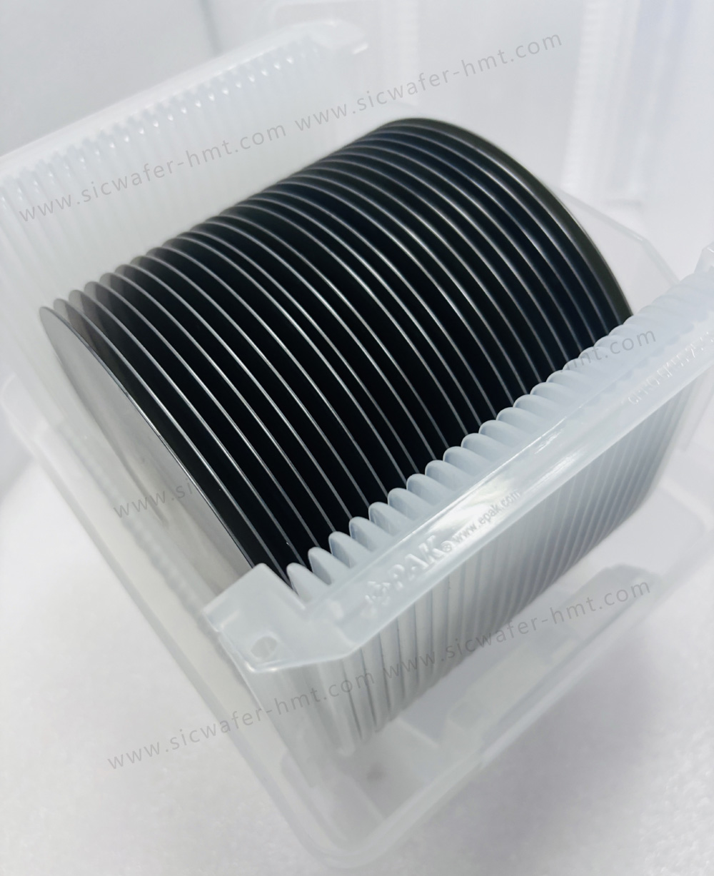
Package: Cassette
Product Description
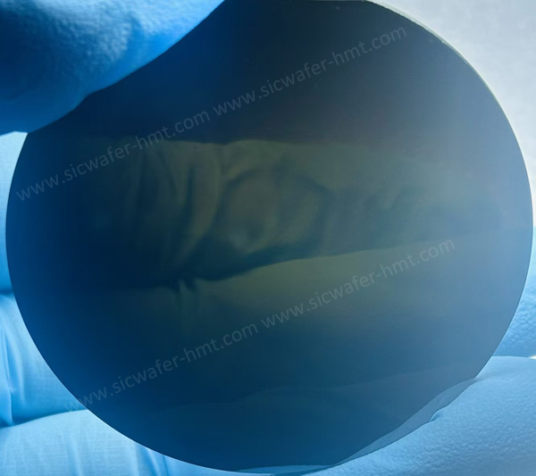
HMT company foucs on Raw cut SiC wafer (As Cut SiC Wafer) manufacture and supply, we supply 2 inch unpolished SiC wafer (Without Grinding SiC Wafer)with thickness 500um 600um 900um 1100um etc. The conductive N type As cut SiC wafer just slicing from SiC Boules, without lapping and polishing process. If customers have different thichness requirements, we also support customized thickness. These unpolished SiC wafers are applied for grinding wheel testing, abrasives testing and so on.
Basic Spec of 2 inch Raw cut SiC wafer
Poly type: 4H
Orientation: 4° toward <11-20> ± 0.5º
Diameter: 50.8±0.38mm
Thickness: 500um 600um 900um 1100um 1200um
Resistivity: 0.15~0.028ohm·cm
Raw-cut 2 inch SiC Wafer

Whether conductive or semi-insulated, the super-smooth surface of the SiC substrate is a necessary condition for its application. The unevenness of SiC surface leads to the increase of dislocation density of homogeneous epitaxial SiC film and heteroepitaxial GaN film, which affects the device performance. The rapid development of the above application fields requires that the surface of SiC wafer can reach the atomic level and the surface is almost free of microscopic defects. The research of ultra-precision SiC wafer flattening technology has extremely important significance for promoting the development of the third generation semiconductor technology.
Related Products


![]() E-mail: kim@homray-material.com ; tina@homray-material.com
E-mail: kim@homray-material.com ; tina@homray-material.com
HMT Gallium Nitride (GaN) Wafer Website: www.ganwafer-hmt.com