

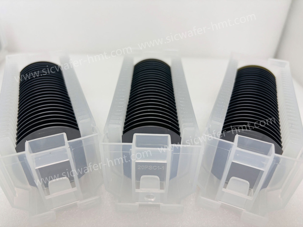
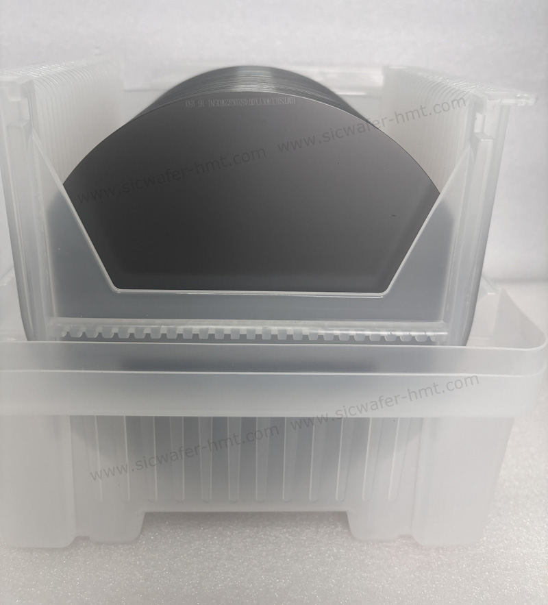
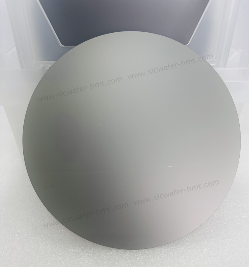
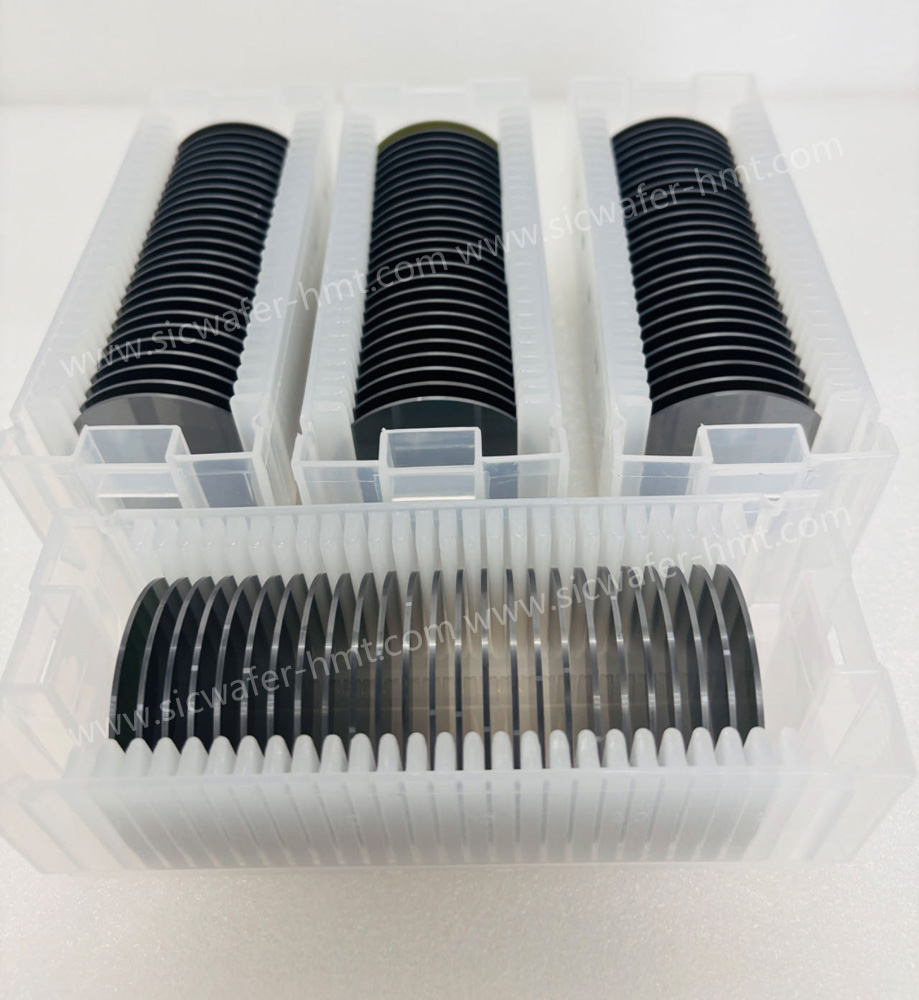
4H-SI Raw-cut SiC Substrate
Diameter: 100mm 150mm
Type: 4H-SI semi-insulating
Thickness: About 600um
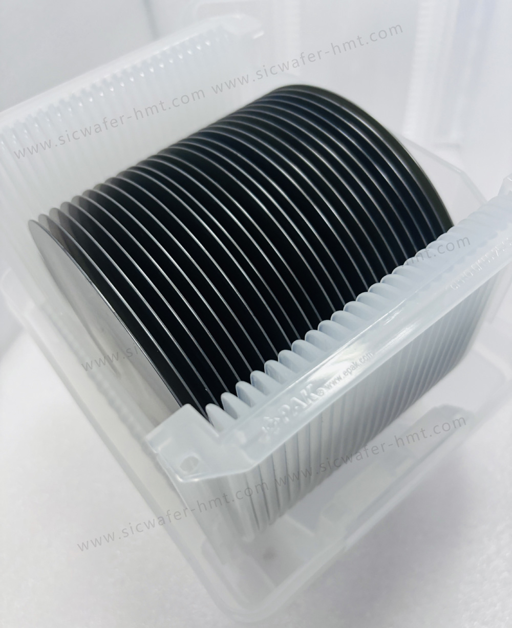
Package: Cassette
Product Description
Find leading SiC As-cut wafer manufacturers in China: HMT supplies premium semi-insulating 4 inch & 6 inch As-cut SiC Substrates. Our raw wafers (unprocessed after ingot slicing) skip lapping/polishing steps – ideal for testing your lapping & polishing equipment. Request inquiry for competitively priced, high-quality as-cut wafers today!
Package of Raw-cut SiC wafer in HMT:


SiC has high energy conversion efficiency, and will not decrease with the increase of frequency, silicon carbide device operating frequency can reach 10 times of silicon based devices, the same specification of silicon carbide MOSFET total energy loss is only 30% of silicon based IGBT. Silicon carbide materials will gradually replace silicon in the fields of high temperature, high frequency and high frequency, and play an important role in 5G communications, aerospace, new energy vehicles and smart power grids.
In high power applications, the third generation semiconductor has wide energy gap, high temperature resistance and high power density characteristics; In high frequency applications, it has the characteristics of low energy consumption and good heat dissipation. Demand for electric vehicles, 5G infrastructure and fast charging are the main growth drivers.
Related Products


![]() E-mail: kim@homray-material.com ; tina@homray-material.com
E-mail: kim@homray-material.com ; tina@homray-material.com
HMT Gallium Nitride (GaN) Wafer Website: www.ganwafer-hmt.com