
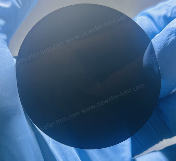
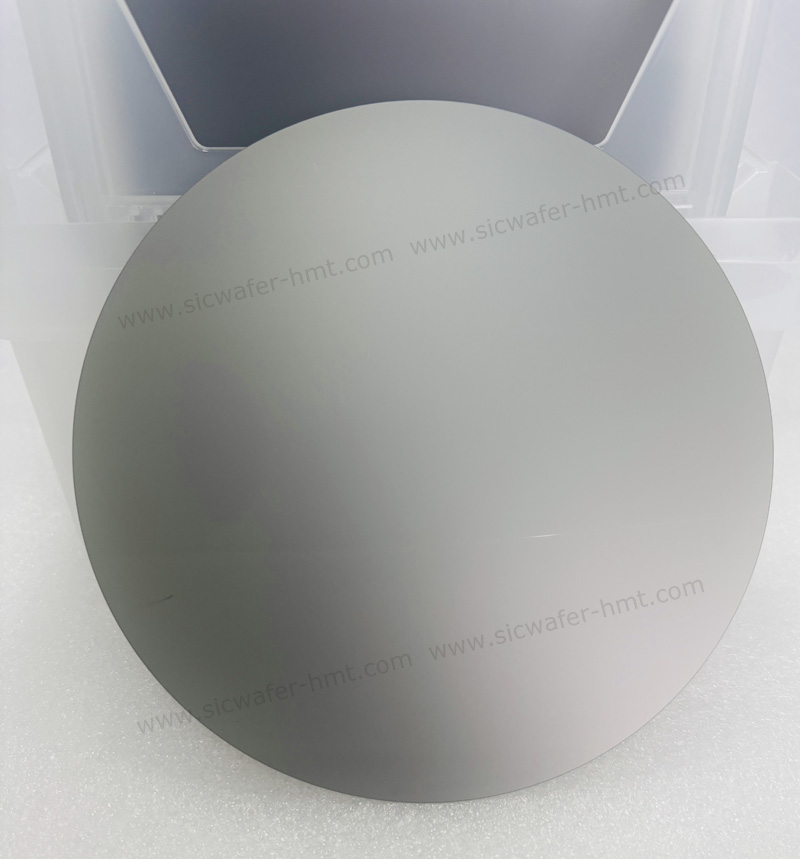
N Type As-cut SiC Wafer 400um Thickness
Diameter: 50.8mm 100mm 150mm
Type: 4H-N Conductive
Thickness: 400um 500um 600um etc
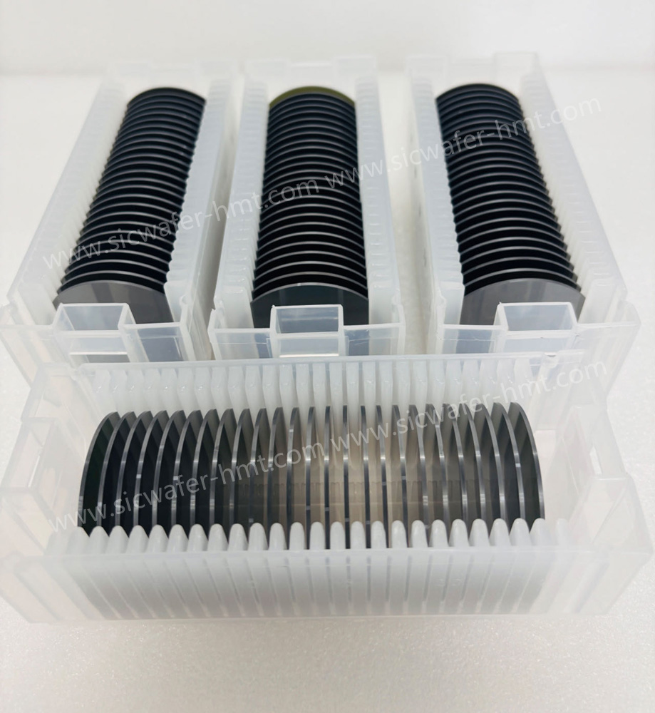
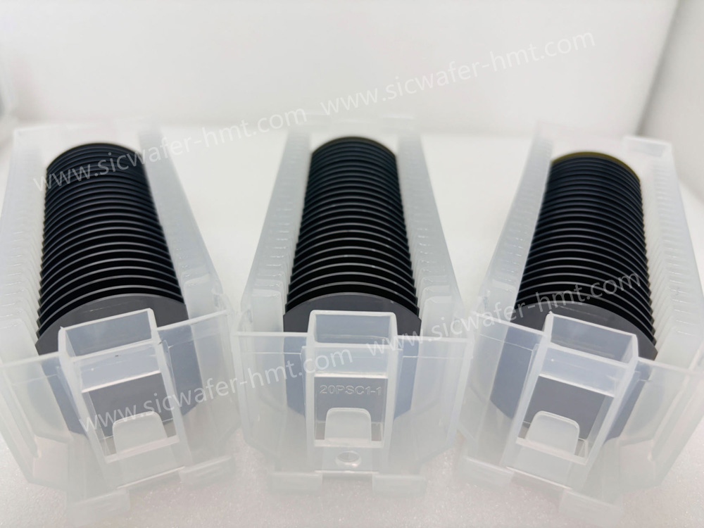
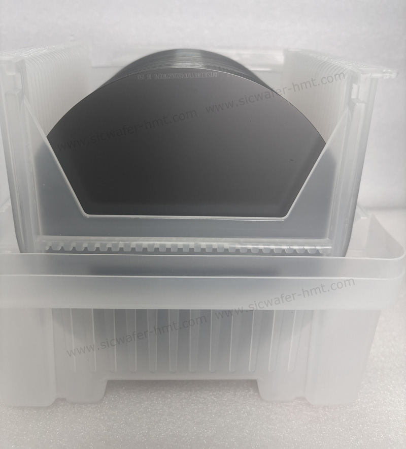
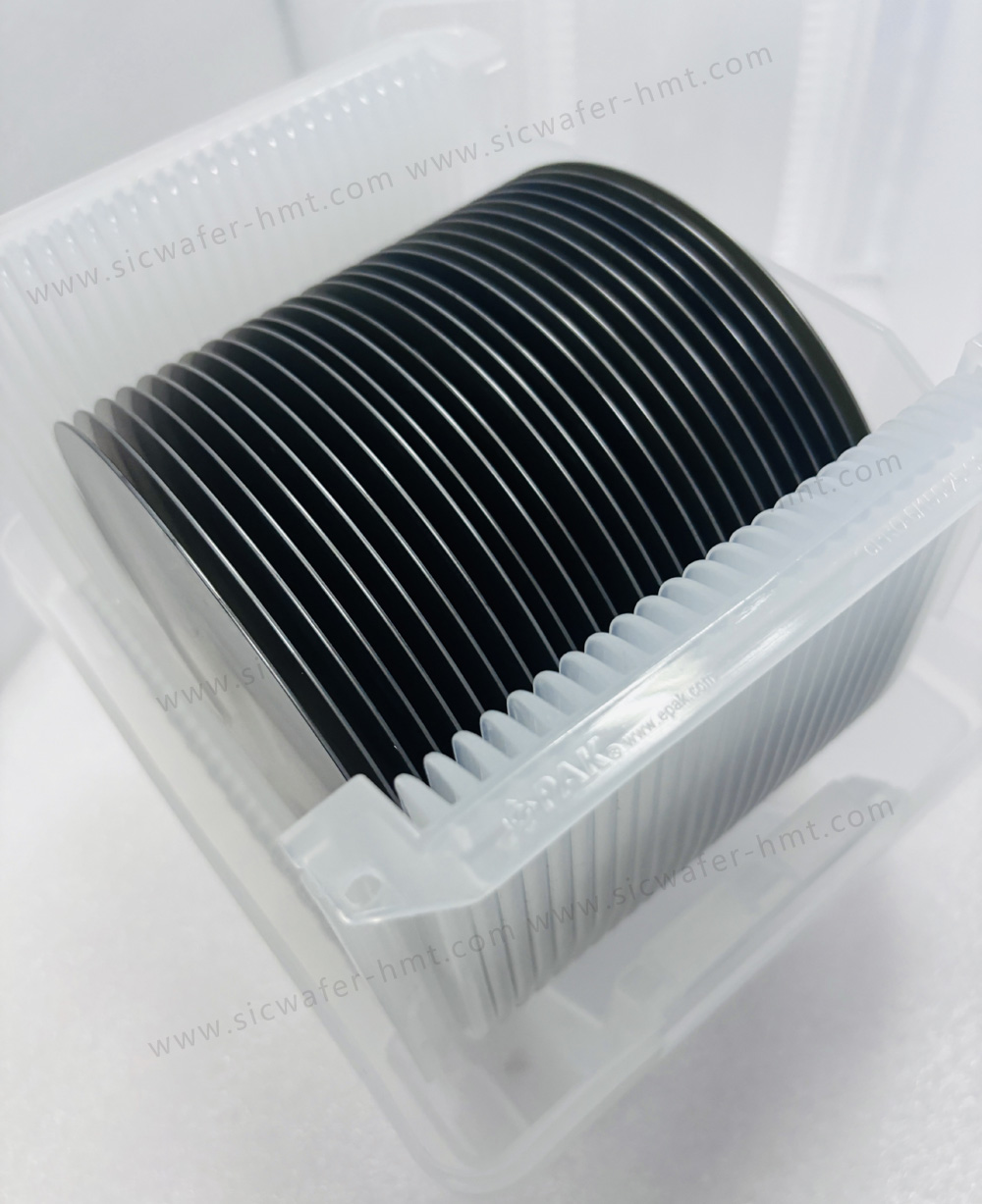
Package: Cassette
Product Description
Purchase lowest MPD As-cut SiC wafer from China HMT company. As-cut SiC Wafer is a 4 inch and 6 inch diameter wafer made from 4H-SiC crystal ingot that is known for its excellent electronic and thermal properties. The as-cut surface of the SiC wafer is a smooth and defect-free surface, making it suitable for a wide range of applications.
The micropipe density of As-cut SiC Wafer is less than 1cm-2, ensuring high reliability and quality. This feature makes it an ideal choice for use in demanding environments and applications that require high-performance materials.
 Product Overview
Diameter: 2 Inch 4 Inch & 6 Inch
Orientation: 4H-SiC
Micropipe Density: < 1cm-2
Type: Conductive N Type
Resistivity: 0.015-0.025 Ohm-cm
As-cut SiC Wafer Packaging Details: Single wafer box or Cassette
To ensure the safe delivery of our products, As-cut SiC Wafers are packaged in cassettes or single wafer box, providing protection from external factors such as dust and moisture. This also allows for easy handling and storage of the wafers.We use Strict Anti-Fragile standard packages.
Silicon carbide (SiC) is a compound semiconductor material composed of carbon and silicon, which is one of the ideal materials for making high temperature, high frequency, high power and high voltage devices. Compared with the traditional silicon material (Si), the band gap of silicon carbide is 3 times that of silicon. The thermal conductivity is 4-5 times that of silicon; The breakdown voltage is 8-10 times that of silicon; The electronic saturation drift rate is 2-3 times that of silicon, which meets the needs of modern industry for high power, high voltage and high frequency. It is mainly used for the production of high-speed, high-frequency, high-power and light-emitting electronic components. The downstream application fields include smart grid, new energy vehicles, photovoltaic wind power, 5G communication, etc. Silicon carbide diodes and MOSFETs have been commercially applied.
Related Products


![]() E-mail: kim@homray-material.com ; tina@homray-material.com
E-mail: kim@homray-material.com ; tina@homray-material.com
HMT Gallium Nitride (GaN) Wafer Website: www.ganwafer-hmt.com