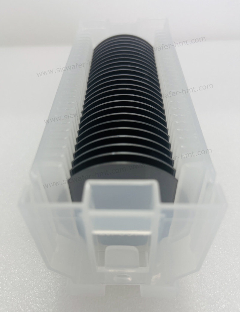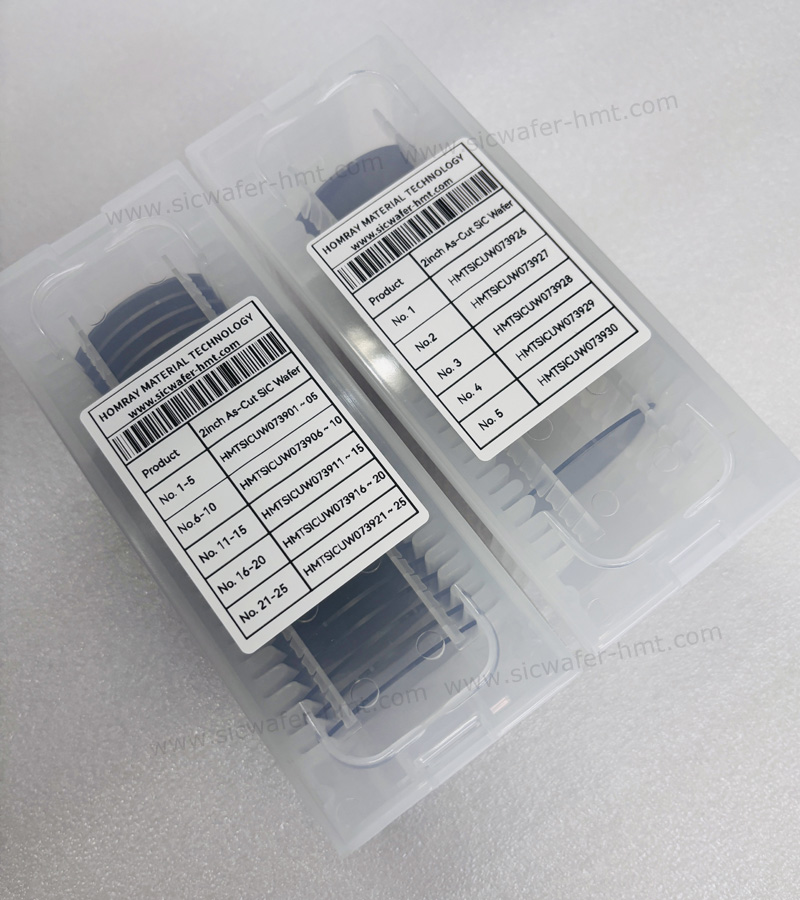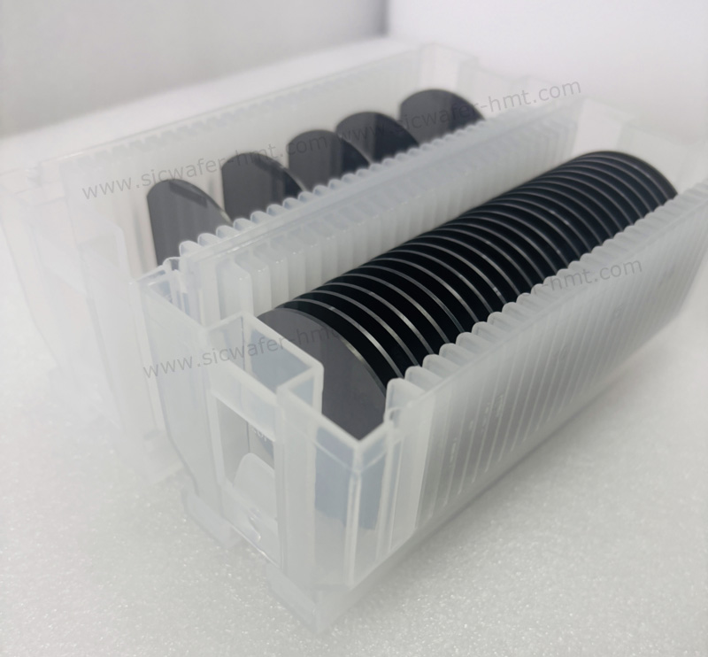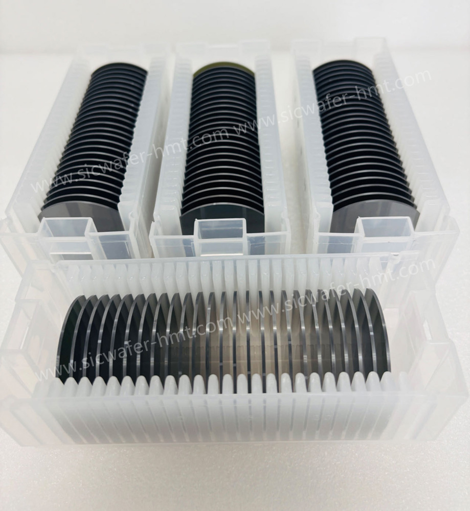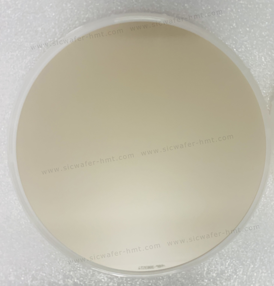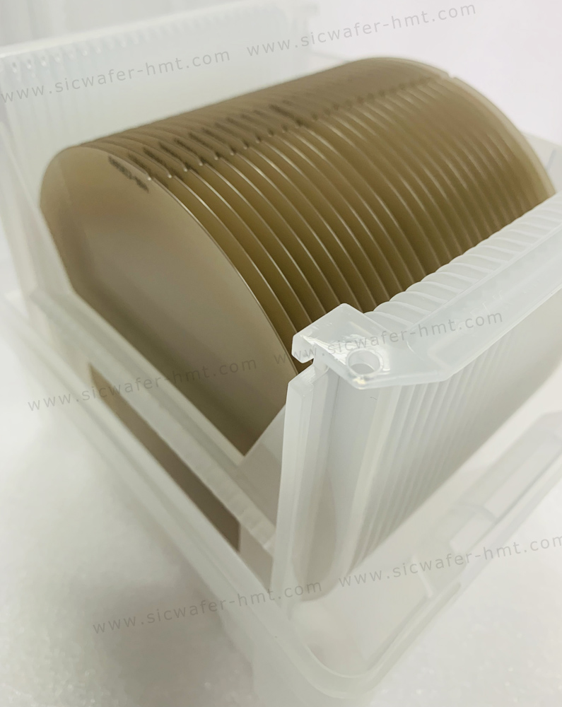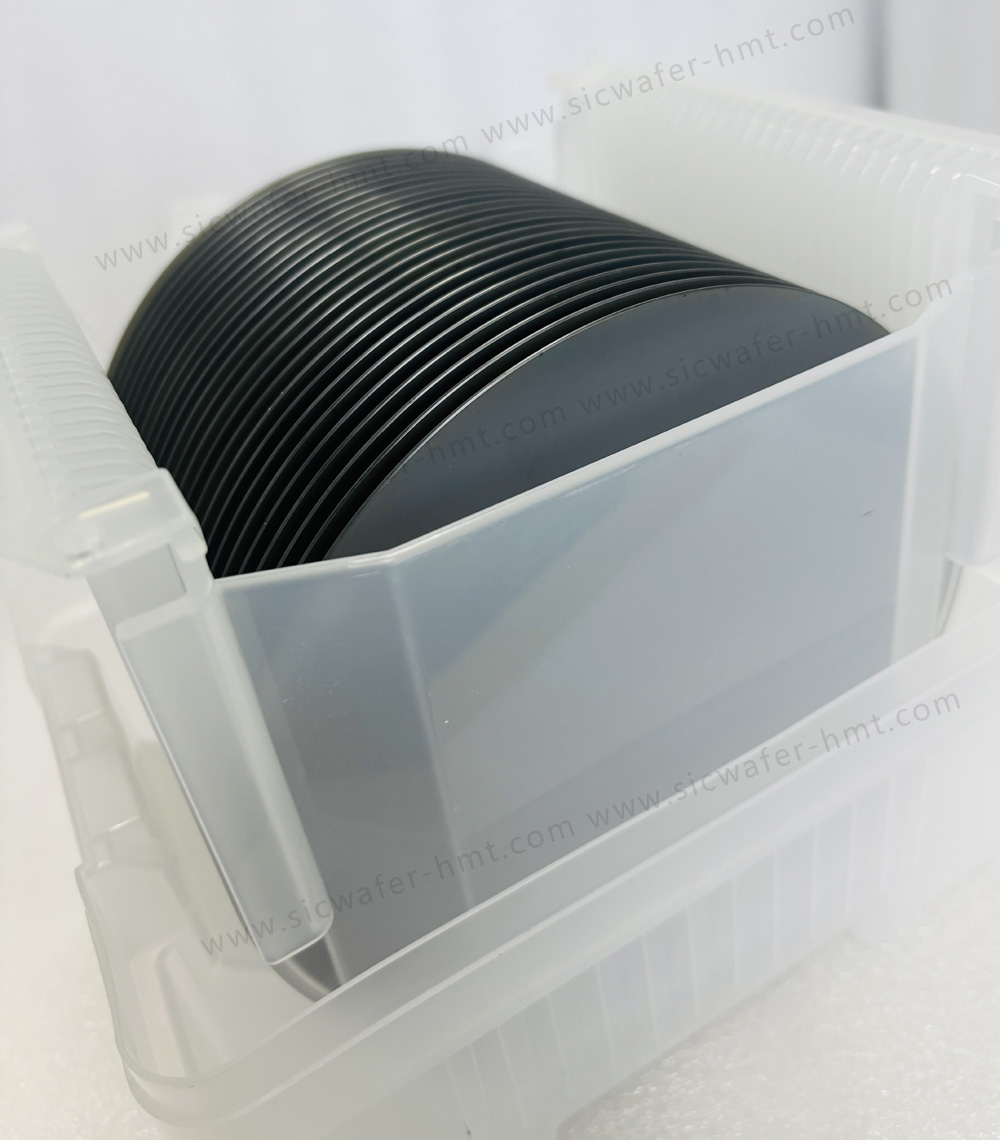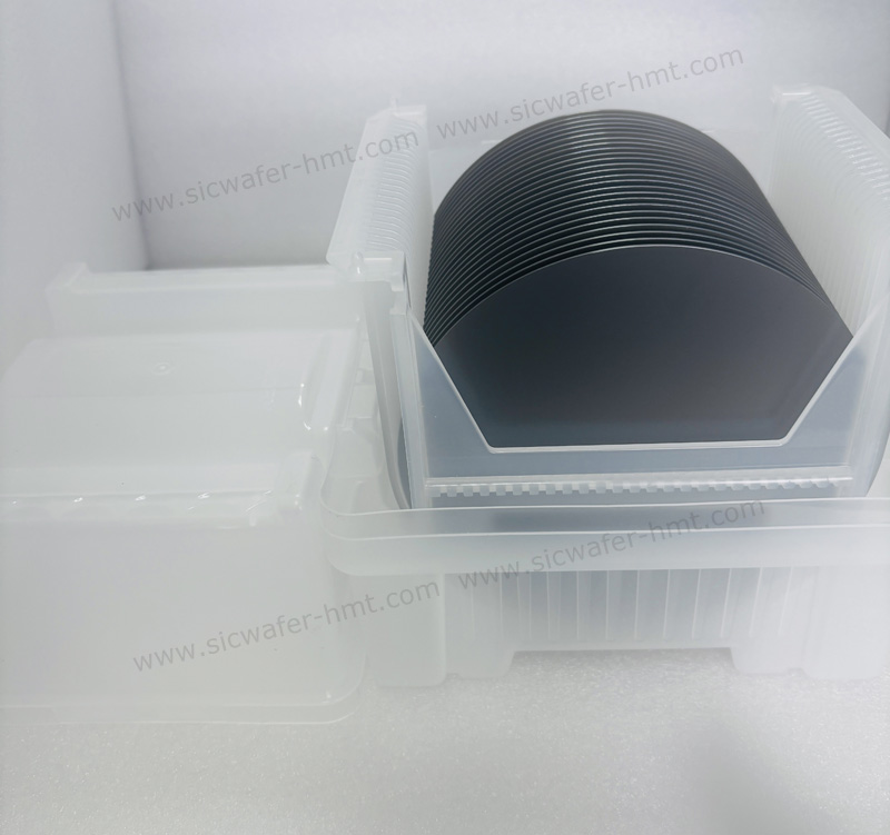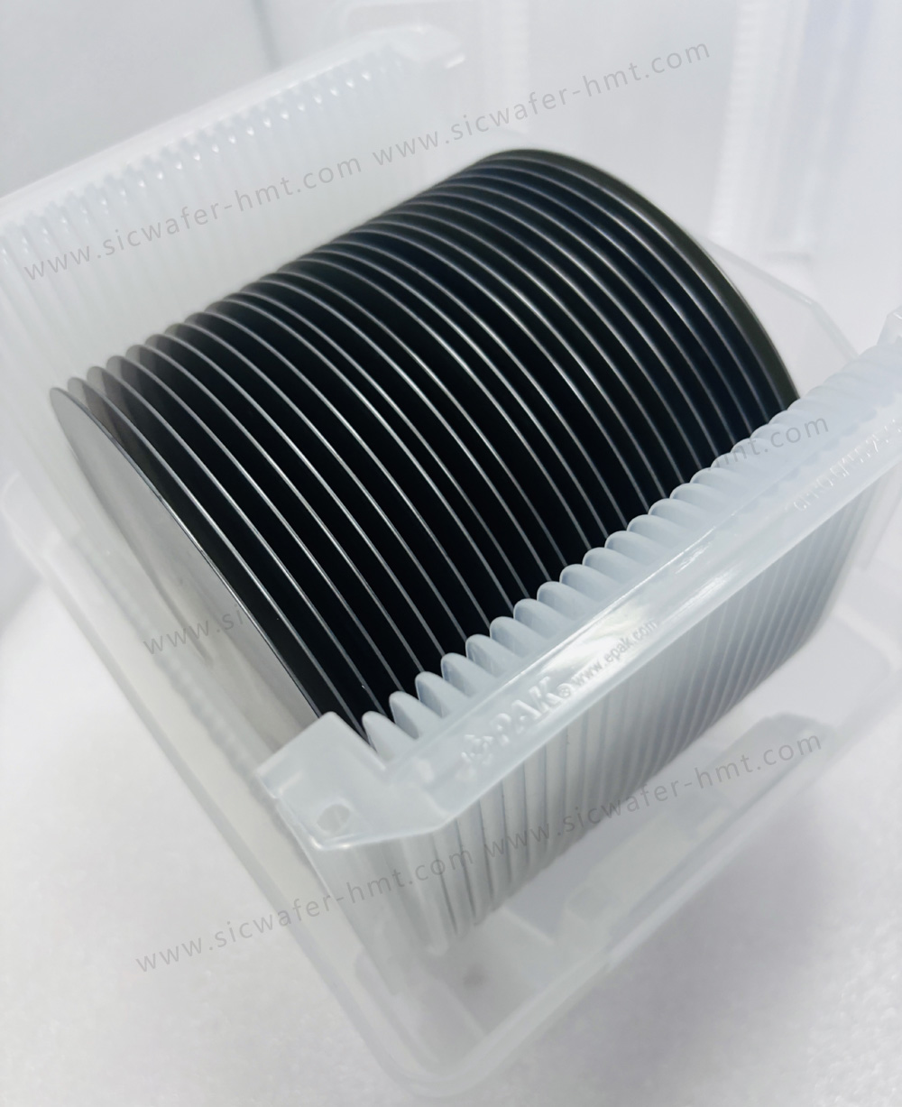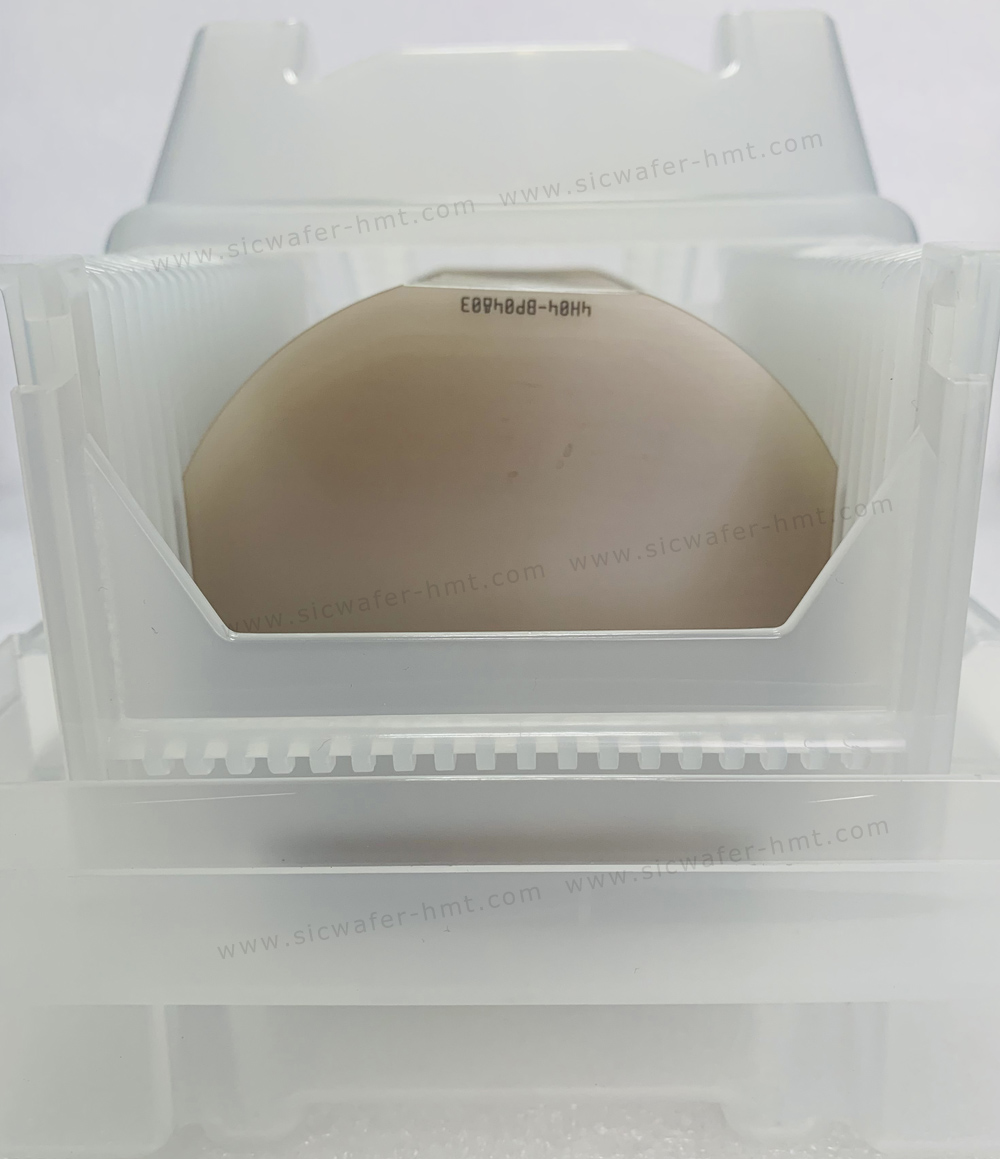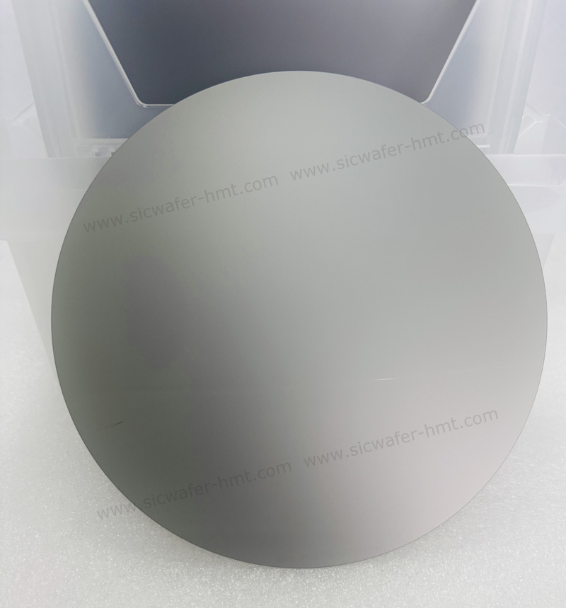
Without Lapping Raw SiC Wafer
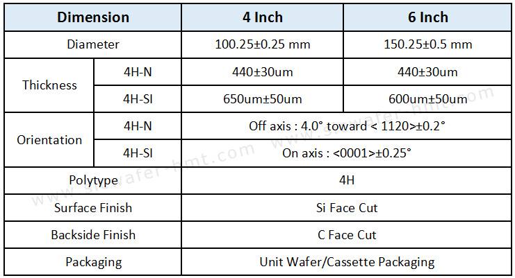
Diameter: 100mm 150mm
Type: 4H-N or 4H-SI
Thickness: About 440um 600um
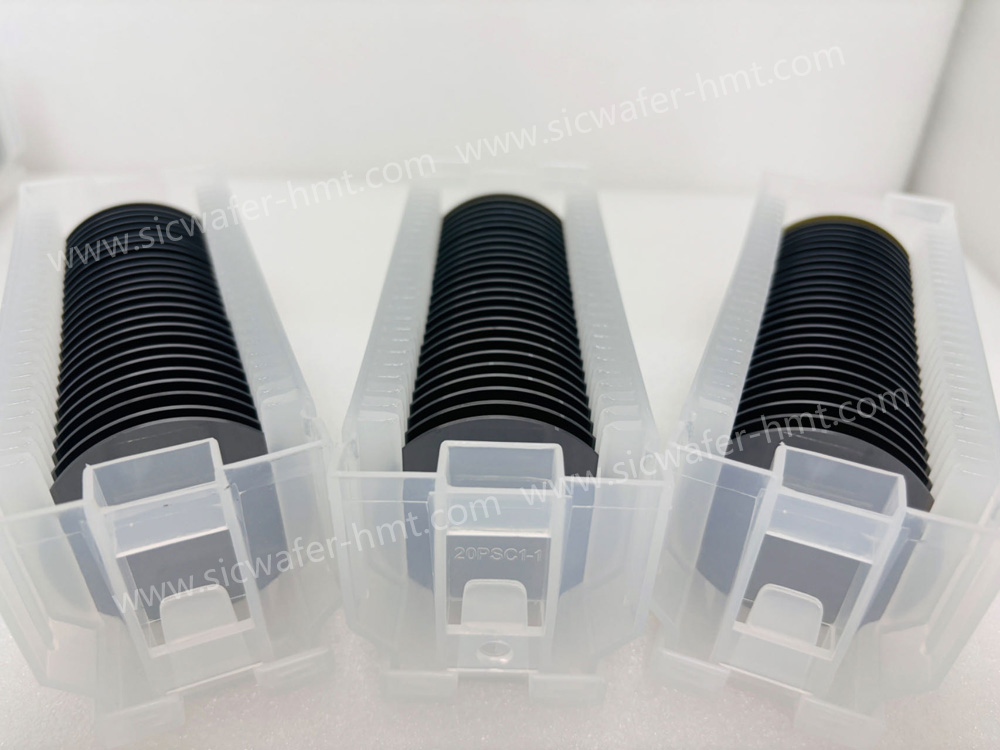
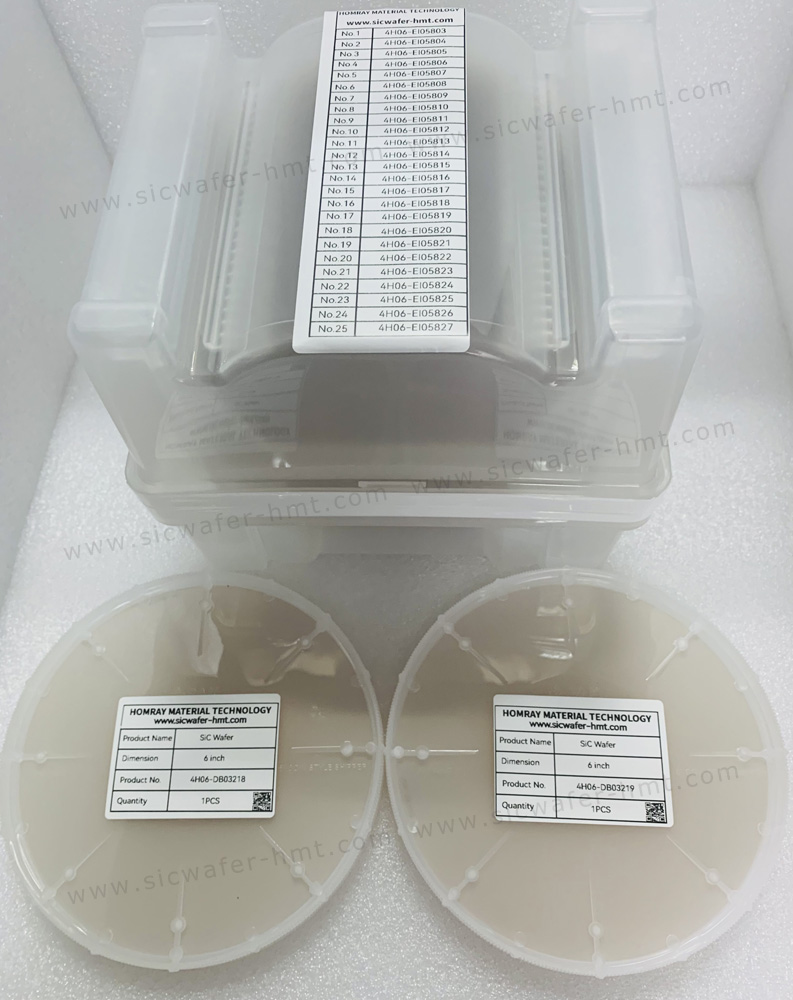
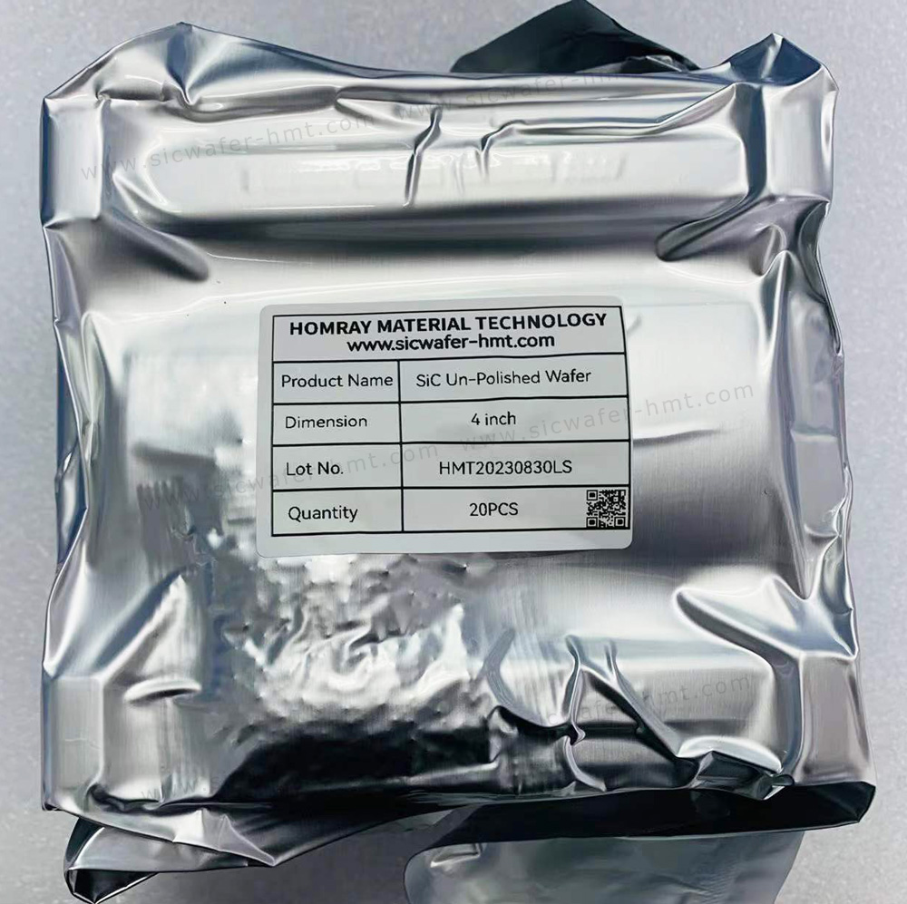
Package: Cassette
Product Description
HMT as guaranteed without lapping raw SiC wafer manufacture and supplier, we manufacture raw SiC wafer for lapping machine testing. The mainstream is 6 inch un-polished raw SiC wafer in the market now. But HMT still keep few 4 inch as-cut SiC wafer capacity allocation for some our customers. Meanwhile, the newest 8 inch without lapping and polishing SiC wafer are available in HMT. Our leadtime of as-cut SiC wafer will be 3~5 weeks upon purchase quantity. Please feel free to contact us for without lapping raw SiC substrate parameters and quotation.
Spec of Un-polished SiC Substrate Wafer
Package of without lapping raw SiC Wafer
SiC substrates can be divided into semi-insulating and conductive types. The semi-insulated substrate mainly achieves the intrinsic high resistivity of the crystal by removing various impurities in the crystal (especially shallow level impurities), while the conductive substrate achieves the low crystal resistivity by introducing nitrogen in the crystal growth process.
The main form of SiC in semiconductors is as a substrate material. SiC e substrate is the cornerstone of GaN and SiC applications in the third generation semiconductor materials. SiC materials mainly grow SiC epitaxial layer on conductive SiC substrate, which is used in all kinds of power devices. In recent years, with the maturity of technology and the decrease of preparation cost, the application of SiC in the field of new energy continues to penetrate.
Related Products


