
HMT is a leading SiC wafer manufacturer, providing high quality 2 inch, 4 inch, 6 inch, and 8 inch SiC as-cut wafers and SiC boules for laser slicing testing. With the widespread application of SiC materials in the semiconductor industry, particularly in electric vehicles, renewable energy, and power electronics, the demand for high-performance SiC wafers continues to grow.Trust HMT, your dedicated SiC wafer manufacturer, to deliver cutting-edge products that enhance production efficiency and meet the evolving needs of the semiconductor industry.
The slicing process of SiC has always been a difficulty in manufacturing. Due to SiC's hardness being second only to diamond and its high brittleness, traditional slicing methods often lead to wafer breakage, material waste, and increased manufacturing costs. Therefore, finding an efficient, low-loss, and fast cutting technology has become key to improving the production efficiency of SiC.
 Advantages of Laser Slicing
Traditional SiC slicing processes usually employ fixed abrasive multi-wire cutting technology. Although this method has been widely used in cutting small-sized SiC, it has several limitations. Firstly, the cutting process consumes a lot of time, especially when the ingot size reaches 8 inches or more, resulting in long cutting cycles, low efficiency, and high costs. Additionally, traditional multi-wire cutting methods have low material utilization, often leading to cutting losses as high as 75%. In the cutting process of high-hardness brittle materials like SiC, surface and subsurface cracks are prone to occur, affecting subsequent grinding and polishing processes.
In contrast, laser slicing technology has the following significant advantages:
High Efficiency and Speed: Laser slicing technology can complete high-precision cutting in a short time. Taking 8-inch SiC as an example, traditional multi-wire cutting takes 10 to 15 days, while laser cutting can control the single-piece cutting time within 20 minutes, significantly improving production efficiency.
-
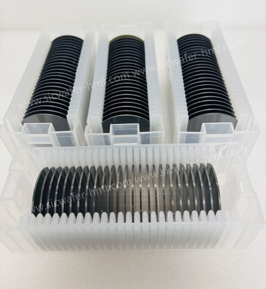
Low Material Loss: Laser slicing technology significantly improves material utilization compared to traditional cutting methods. The loss from laser cutting is only about 60 microns, whereas traditional cutting losses are as high as 75%. Through laser cutting, a single 20 mm SiC ingot can produce more than 50 wafers, and in some cases, even up to 80 wafers, greatly reducing material waste.
-
High Yield: Laser slicing technology can increase the production yield. Compared to traditional cutting methods, laser slicing can produce more wafers in a shorter time. For large-sized SiC ingots (such as 8-inch), using laser slicing can significantly improve production efficiency and yield, thereby reducing unit product costs.
-
Clean and Environmentally Friendly: The laser cutting process does not require diamond abrasives or grinding fluids, avoiding the dust and wastewater pollution issues associated with traditional cutting methods. Laser cutting is a cleaner processing method, contributing to improved environmental friendliness.
![]() M.P: +86-15366208370 ; +86-15366203573
M.P: +86-15366208370 ; +86-15366203573
![]() E-mail: kim@homray-material.com ; tina@homray-material.com
E-mail: kim@homray-material.com ; tina@homray-material.com
HMT Gallium Nitride (GaN) Wafer Website: www.ganwafer-hmt.com