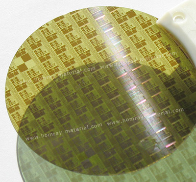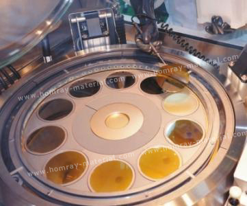
Epitaxial layer is based on wafer, through epitaxial process to grow a specific single crystal film, substrate wafer and epitaxial film together called epitaxial sheet. The SiC Epitaxial layer is grown on the conductive SiC substrate to prepare the SiC homogeneous epitaxial sheet, which can be further made into Schottky diodes, MOSFETs, IGBTs and other power devices, among which 4H-SiC substrate is the most used.
HMT company not only provide SiC substrates but also produce high quality SiC Epi Wafer from 4 inch to 6 inch for Schottky diodes, MOSFETs, JFETs, and BJTs over a wide voltage range for green energy systems such as solar inverters, wind farm, hybrid and electric vehicles, and numerous other energy-efficient systems.The main preparation methods of SIC Epitaxial layer are: evaporation growth method; Liquid phase epitaxial growth (LPE); Molecular beam epitaxial growth (MBE); Chemical vapor deposition (CVD). Chemical vapor deposition (CVD) is the main method for mass production in factories.


Because the SiC power device is different from the traditional silicon power device manufacturing process, it can not be directly made on the SiC ingle crystal material, and must grow additional high-quality epitaxial materials on the conduction type single crystal substrate, and manufacture all kinds of devices on the epitaxial layer, so the quality of epitaxial has a great impact on the performance of the device. The improvement of performance of different power generators also puts forward higher requirements for the thickness of epitaxial layer, doping concentration and defects.