SiC material has wide band gap, high breakdown electric field, high thermal conductivity, high electron mobility and radiation resistance, SiC based SBD and MOSFETs are more suitable for high frequency, high temperature, high pressure, high power and radiation resistance environment. With the same power level, the SiC device can meet the requirements of higher power density and more compact design. SiC material has wide band gap, high breakdown electric field, high thermal conductivity, high electron mobility and radiation resistance, SiC based SBD and MOSFETs are more suitable for high frequency, high temperature, high pressure, high power and radiation resistance environment. With the same power level, the SiC device can meet the requirements of higher power density and more compact design.
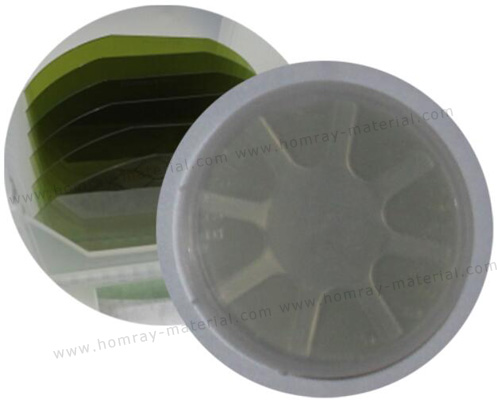
Homray Material Technology as the leading manufacturer and supplier of SiC material, we supply 4 inch N type SiC Ingot, 4 inch SiC substrate wafer with N type and SI type, 6 inch SiC wafer and ingots and 8 inch conductive SiC substrate. Choose HMT company, get lower quotation, contact us now.


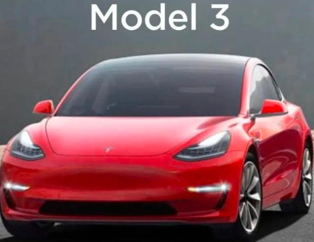
Silicon carbide SiC has a higher power density than traditional silicon wafers, making the size and volume of devices smaller and the corresponding battery size smaller, thus extending battery life and giving electric cars longer range. Tesla's Model 3, for example, uses silicon carbide instead of silicon for its current conversion module.
The main form of silicon carbide in semiconductors is as a substrate material. SiC e substrate is the cornerstone of GaN and SiC applications in the third generation semiconductor materials. SiC materials mainly grow silicon carbide epitaxial layer on conductive SiC substrate, which is used in all kinds of power devices. In recent years, with the maturity of technology and the decrease of preparation cost, the application of silicon carbide in the field of new energy continues to penetrate.