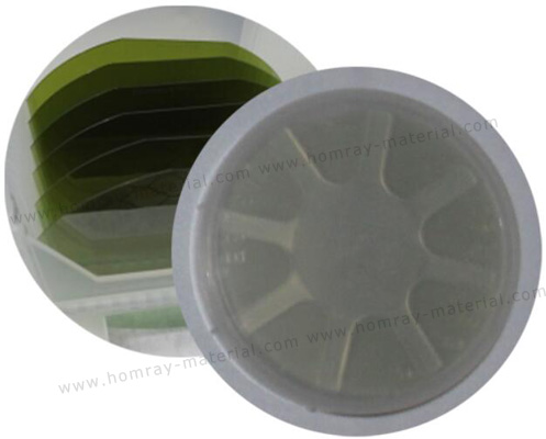
 SiC substrate is the cornerstone of GaN and SiC application in the third generation semiconductor materials. Due to the limitation of technology and process level, large-scale application of GaN material as substrate is still facing challenges. Its application mainly uses sapphire, silicon wafer or semi-insulating SiC wafer as substrate, and fabricate GaN devices by epitaxy growth, which is mainly used in the field of macro station communication radio frequency. The silicon carbide material is mainly in the conductive N type SiC substrate epitaxial growth SiC epitaxial layer, should be used in all kinds of power devices, in recent years, with the maturity of technology and preparation cost, the application in the field of new energy continues to penetrate. Silicon carbide material will be the important foundation of silicon carbide and gallium nitride devices in the fields of new energy and 5G communication.
HMT produces 4H-SiC wafer with best price. We have different grade of SiC wafer to meet your project requirement. HMT has a complete SiC(silicon carbide) wafer substrate production line integrating crystal growth, crystal processing, wafer processing, polishing, cleaning and testing. HMT keeps focusing on semi-conductive technology development, and accredit by Market and Government with our efforts. Any questions feel free to contact us,we'll fully support your project.
SiC material has a wide band gap, high breakdown electric field, high thermal conductivity, high electron mobility and radiation resistance characteristics, SiC based SBD and MOSFET is more suitable for high-frequency, high temperature, high pressure, high power and radiation resistance in the environment. Under the condition of the same power level, the use of SiC devices can reduce the volume of electric drive, electronic control, etc., to meet the demand of higher power density, more compact design, but also can make the electric vehicle longer range. On the one hand, SiC power components are gradually mature in terms of technology, on the other hand, the trend of intelligent and electrification continues to evolve, and the upgrade of downstream traditional vehicles brings huge demand for power semiconductor, so there is a wide space for replacing SiC power devices.
The breakdown field strength of SiC insulation is 10 times that of Si, so compared with Si devices, it can produce high voltage power devices of 600V ~ thousands of V with higher impurity concentration and thinner drift layer. The impedance of high voltage power devices is mainly composed of the impedance of the drift layer, so using SiC can get very low conduction resistance per unit area of high voltage devices. Theoretically, the same voltage withstand device, the unit area of SiC drift layer impedance can be reduced to Si 1/300.