 Electric vehicles and 5G infrastructure drive the demand for power components, and the third generation semiconductor plays an important role. Major countries such as China and the United States have promoted policies, and enterprises at home and abroad are also rushing to invest. Industry analysts say SiC substrates are the biggest key to development.
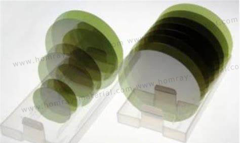
Homray Material Technology offers 100mm and 150mm 4H-SiC substrate wafer with Conductive N type & Semi-insulating type to meet your project requirement. Customized SiC Substrate thickness or orientation are also available in HMT with favourable price. Please contact us today by email to discuss your project requirements.
The third generation semiconductor uses Silicon Carbide (SiC) and Gallium Nitride (GaN) as the main materials, which is different from the first generation semiconductor which uses Silicon (Si) and Germanium (Ge) as the main materials, and the second generation semiconductor uses Gallium Arsenide (GaAs), Indium Phosphide (InP) and Aluminum Gallium Arsenide (AlGaAs) as the main materials.
SiC substrate manufacturing is quiet difficult, the main reason is the high cost. The thermal field control and crystal seed control are quite key, but can only be native steelmaking, doing the process of learning, learning the process of doing. SiC long crystal efficiency is 100 to 200 times slower than Si, Si long crystal about 3 days to make 200 cm high crystal bar, SiC to 7 days to grow 2 to 5 cm crystal ball. In addition, SiC hard and brittle, cutting, grinding and polishing difficulty is high, there will be a lot of waste.
In high power applications, the third generation semiconductor has wide energy gap, high temperature resistance and high power density characteristics; In high frequency applications, it has the characteristics of low energy consumption and good heat dissipation. Demand for electric vehicles, 5G infrastructure and fast charging are the main growth drivers.