
HMT specializes in producing 4H-polytype silicon carbide (SiC) crystal ingots and SiC substrates, available in both semi-insulating (un-doped) and N-type conductivities. Processed from these ingots, SiC substrates provide an ideal platform for power electronics, offering key benefits such as low on-resistance, high breakdown voltage, excellent thermal conductivity, and high-temperature operation. These properties contribute to reduced switching losses, lower cooling demands, and enable more compact, lightweight, and high-performance system designs.
① Raw Material Synthesis
High-purity silicon powder and high-purity carbon powder are uniformly mixed according to the process formula. Under high-temperature conditions exceeding 2000°C in a reaction chamber and through specific reaction processes, trace impurities remaining in the reaction environment and adsorbed on the surface of the reaction micropowder are removed. This allows the silicon and carbon powders to react and synthesize silicon carbide particles with specific crystal types and particle sizes according to the predetermined stoichiometric ratio. Subsequent processes such as crushing, sieving, and cleaning are then carried out to produce high-purity silicon carbide powder raw materials that meet the requirements for crystal growth. Each batch is sampled and tested for purity, particle size, etc.
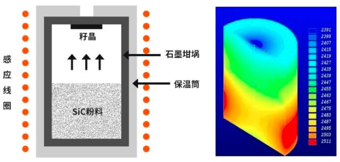
② Crystal Growth
SiC crystal growth methods include Physical Vapor Transport (PVT), High-Temperature Chemical Vapor Deposition (HTCVD), and the Liquid Phase Method. Considering factors such as growth condition control, growth efficiency, and defect control, the Physical Vapor Transport method is the most technologically mature and widely used. The other two methods are still in the research and development stage. Major foreign silicon carbide wafer manufacturers such as Wolfspeed, Coherent, and SiCrystal all employ the Physical Vapor Transport method.
③ Ingot Processing
The SiC ingot is oriented using an X-ray single crystal orientation instrument. It is then ground flat and rounded through precision mechanical processing to form a silicon carbide crystal rod with standard diameter dimensions and angles. All formed crystal rods are inspected for dimensions, angles, and other indicators.
④ Slicing
Considering the allowance for subsequent processing, the SiC crystal rod is sliced into substrates of varying thicknesses to meet customer requirements using diamond wire sawing. Fully automatic testing equipment is then used to inspect the wafer geometry, including warp, bow, and total thickness variation (TTV).
⑤ Lapping
The wafer is lapped to the required flatness and roughness using diamond slurries with different particle sizes. This process also eliminates surface wire marks and damage. All sliced wafers are tested for geometry and electrical properties using fully automatic testing equipment and non-contact resistivity testers.
⑥ Polishing
The polishing process for silicon carbide wafers can be divided into rough polishing and fine polishing. Rough polishing is mechanical polishing, aimed at improving polishing efficiency. A key research direction for mechanical polishing of silicon carbide single crystal substrates is optimizing process parameters to improve wafer surface roughness and increase the material removal rate. Fine polishing is single-side polishing. Chemical Mechanical Polishing (CMP) is the most widely used polishing technology. It achieves material surface removal and planarization through the synergistic action of chemical corrosion and mechanical abrasion. The wafer undergoes an oxidation reaction under the action of the polishing slurry, generating a softened layer that is relatively easily removed by the mechanical action of abrasive particles. As the final process in single crystal substrate processing, Chemical Mechanical Polishing is a common method for achieving global planarization of silicon carbide substrates and is also a key process for ensuring an ultra-smooth, defect-free surface on the processed substrate.
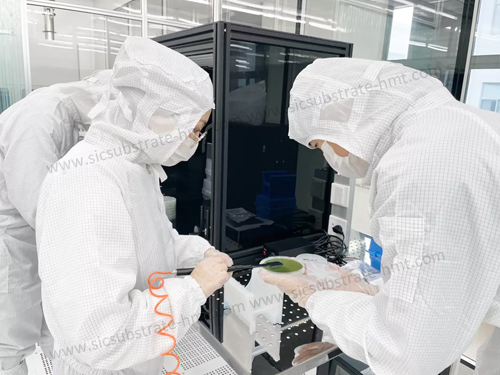
⑦ Inspection
Instruments such as optical microscopes, X-ray diffractometers, atomic force microscopes, non-contact resistivity testers, surface flatness testers, and comprehensive surface defect testers are used to inspect various parameter indicators of the silicon carbide wafers. These include micropipe density, crystalline quality, surface roughness, resistivity, warp, bow, total thickness variation (TTV), and surface scratches. Based on these, the quality grade of the wafer is determined.
⑧ Cleaning
The polished SiC Substrate are cleaned with cleaning agents and pure water to remove microscopic dust particles, metal ions, organic contaminants, etc., from the wafer surface. They are then dried using ultra-high purity nitrogen and a spin dryer. The wafers are finally packaged in clean cassettes in a cleanroom environment, forming SiC wafers ready for immediate use by downstream customers.
![]() E-mail: kim@homray-material.com ; tina@homray-material.com
E-mail: kim@homray-material.com ; tina@homray-material.com
HMT Gallium Nitride (GaN) Wafer Website: www.ganwafer-hmt.com