
SiC Optical Waveguide for AR Glasses: How Silicon Carbide Enables Wider FOV
Silicon carbide (SiC) is emerging as a high-index substrate for next-generation AR optical waveguides because its optical and thermal properties address several limitations of conventional glass and polymer waveguides. Its high refractive index can support wider-field optical designs, while its thermal conductivity and mechanical stability provide additional advantages for compact AR systems and precision grating fabrication.
Why Does AR Optical Waveguide Need a High Refractive Index?
 AR optical waveguides guide image light from a microdisplay into the user's eye through a combination of optical coupling, propagation and out-coupling. In many diffractive waveguide architectures, light is introduced through an in-coupling structure, propagates through the substrate and is repeatedly confined before being extracted toward the eye.
A fundamental principle behind this light confinement is total internal reflection (TIR). When light travels inside a higher-refractive-index material toward an interface with a lower-index medium such as air, it can remain confined when the incidence angle exceeds the critical angle.
The refractive index of the waveguide therefore directly influences the angular range over which light can be guided. A higher-index substrate can provide greater design freedom for compact waveguide systems, although the final field of view also depends on grating geometry, coupling efficiency, wavelength, optical losses and display architecture.
For a simplified single-projection geometry, a commonly used theoretical relationship can be expressed as:
FOV limit ≈ 2 × arcsin(n) − 90°
where n represents the refractive index of the waveguide material under the simplified assumptions of the mo
oximately 1.5 provides a much narrower theoretical angular range than a material with an index approaching or exceeding 2.0.
The practical FOV of a commercial AR system should not, however, be calculated from refractive index alone. Grating pitch, diffraction efficiency, pupil expansion, color management, eye box, display characteristics and optical losses all contribute to the final system-level FOV.
Why Is Silicon Carbide Attractive for AR Optical Waveguides?
High Refractive Index
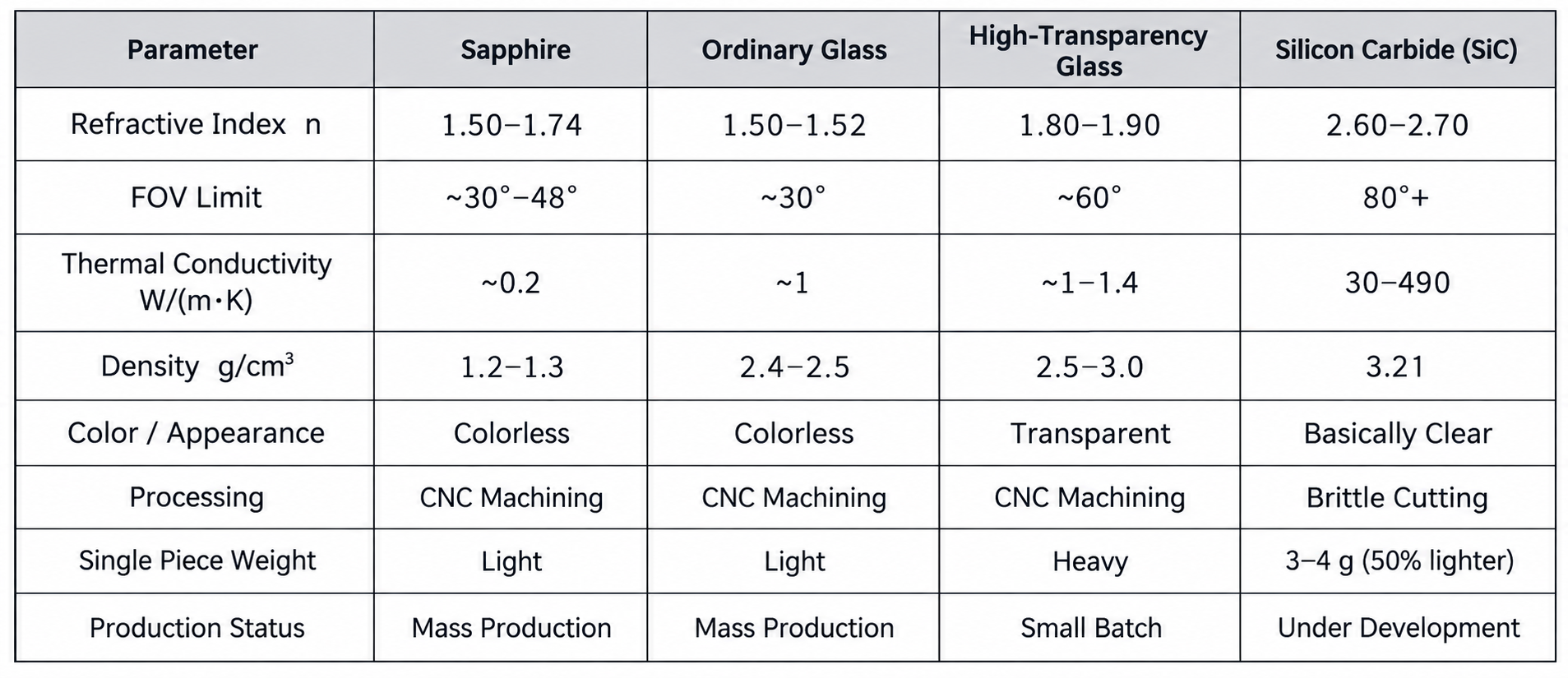
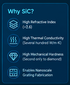 Optical-grade SiC can provide a refractive index above 2.6 in relevant visible wavelengths, depending on wavelength, crystal structure and material conditions. This places SiC well above many conventional polymer waveguide materials and makes it attractive for compact high-index optical designs.
The importance of this property is straightforward: a higher refractive index can increase the angular range available for waveguide propagation and therefore provide a pathway toward wider FOV designs.
The actual FOV of an SiC AR waveguide still depends on the complete optical architecture. SiC should therefore be considered an enabling substrate rather than a guarantee of a specific FOV.
Thermal Conductivity
SiC also offers a major thermal-management advantage. High-quality single-crystal SiC can exhibit thermal conductivity on the order of several hundred W/(m·K), substantially higher than ordinary glass.
For AR glasses, this property can become important because Micro-LED projectors, laser or other optical engines, electronics and compact computing components generate heat inside a very limited volume.
A SiC optical substrate can potentially participate in heat spreading instead of functioning only as a passive optical element. The practical thermal performance of a finished waveguide, however, depends on crystal quality, processing, coatings, bonding layers and the overall optical-mechanical structure.
Mechanical Hardness and Structural Stability
SiC is an extremely hard ceramic material, which creates both an advantage and a manufacturing challenge.
Its mechanical strength and hardness can provide excellent structural stability for thin optical components, but conventional mechanical or nanoimprint approaches designed for softer materials are not necessarily directly transferable to SiC.
This has encouraged the use of semiconductor-style lithography, plasma etching and other precision processes for creating nanoscale optical structures directly on SiC substrates.
How Can SiC Help Reduce Rainbow Artifacts?
Rainbow artifacts are one of the important optical challenges associated with diffractive AR waveguides. They can arise because different wavelengths of visible light interact differently with nanoscale grating structures, producing unwanted color separation or stray-light effects under certain viewing conditions.
A higher-index substrate can provide greater freedom in designing grating pitch, geometry and diffraction conditions. This can help engineers manage the angular distribution of different wavelengths and design the optical stack to reduce unwanted visible artifacts.
SiC is therefore attractive not simply because it has a high refractive index, but because that index can be combined with precision diffractive structures in a compact optical substrate.
Meta's Orion AR glasses provide a high-profile industry example. Meta states that Orion combines Micro LED projectors with optical-grade silicon carbide and achieves an approximately 70° field of view. Meta also describes its optical-grade SiC development as helping minimize stray-light effects such as rainbow artifacts.
For the broader industry, this demonstrates that SiC is moving beyond a theoretical materials discussion and into practical AR optical development.
SiC and Semiconductor-Grade Grating Fabrication
The hardness of SiC makes precision fabrication particularly important for optical waveguide applications.
A typical SiC waveguide manufacturing route can involve:
SiC crystal → wafer slicing → surface preparation → polishing → lithography → plasma etching → nanoscale grating → optical inspection
The objective is to create tightly controlled grating structures with the required pitch, depth, sidewall profile and dimensional uniformity.
Semiconductor-grade etching offers a significant process advantage because it can directly transfer nanoscale patterns into the SiC surface. Compared with polymer-based structures, etched SiC gratings can provide strong dimensional stability and avoid some of the long-term deformation or aging mechanisms associated with organic imprint materials.
The exact process depends on the waveguide architecture. Grating depth, aspect ratio, sidewall angle, surface roughness and etch selectivity must all be controlled according to the target wavelength and optical design.
SiC Waveguide Thermal Management for Micro-LED AR Systems
The development of high-brightness AR displays creates another reason to consider SiC.
Micro-LED optical engines can deliver high brightness within a very compact package, but the resulting heat must be managed without increasing the size or weight of the glasses.
A conventional optical waveguide mainly serves as a light-guiding element. A SiC waveguide creates the possibility of combining optical and thermal functions within the same substrate.
Heat generated near the optical engine can potentially spread through the SiC component and toward the frame or other thermal-management structures. This approach can help reduce local temperature accumulation and may support stable operation under demanding brightness conditions.
The effectiveness of this approach depends on the complete stack rather than the substrate alone. Bonding layers, coatings, grating structures, mounting methods and thermal interfaces can all affect the final thermal resistance.
HMT 4H-HPSI SiC Substrates for Optical and AR Applications
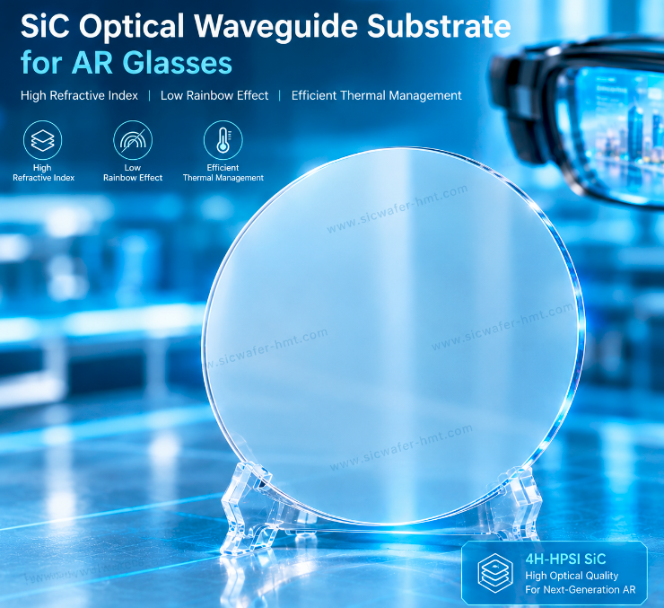
HMT supplies 4H-HPSI SiC substrates for AR lens and optical applications, providing a SiC material platform for customers developing high-index optical components and emerging AR waveguide technologies.
The available substrate configurations include 4-inch, 6-inch and 8-inch formats, depending on the product specification and application requirements.
For applications requiring controlled wafer thickness and surface preparation, substrate parameters can be selected according to downstream lithography, etching, polishing and optical-processing requirements.
For more information, see our 4H-HPSI SiC substrates for AR lenses.
For larger-area substrate requirements, HMT also provides 8-inch HPSI SiC substrate wafers for semiconductor and emerging optical-material applications.
The broader HMT product range includes different SiC wafer grades, crystal types and wafer dimensions for semiconductor and advanced-material applications. See our SiC wafers and substrates for additional product configurations.
From SiC Crystal to Optical Waveguide Substrate
The performance of an SiC optical component begins with the quality of the starting crystal.
SiC crystal growth is followed by processes such as boule preparation, wafer slicing, lapping, polishing, cleaning and inspection. Each stage can influence the final wafer geometry and surface condition.
For optical waveguide applications, the substrate must provide a suitable foundation for nanoscale patterning. Parameters such as thickness uniformity, surface roughness, TTV and wafer flatness can therefore become important during process development.
The relationship can be summarized as:
SiC Crystal → Wafer → Surface Preparation → Precision Patterning → Diffractive Waveguide → AR Optical System
This process chain also explains why SiC wafer suppliers with semiconductor-material processing experience can play an important role in the development of next-generation optical components.
FAQ
What is a SiC optical waveguide?
A SiC optical waveguide is an optical component or substrate based on silicon carbide that guides light through mechanisms such as total internal reflection and diffractive coupling. Its high refractive index makes SiC attractive for compact AR waveguide architectures.
Why is SiC used for AR optical waveguides?
SiC combines a high refractive index with high thermal conductivity and exceptional mechanical hardness. These properties can support wider-FOV optical designs, thermal management and precision fabrication of nanoscale diffractive structures.
What refractive index does SiC provide for AR waveguides?
Optical-grade SiC can provide a refractive index above 2.6 in relevant visible wavelengths, depending on wavelength, crystal structure and material conditions. The exact optical parameters should be evaluated for the specific SiC grade and waveguide architecture.
 E-mail: kim@homray-material.com ; tina@homray-material.com
HMT Gallium Nitride (GaN) Wafer Website: www.ganwafer-hmt.com